Electronic circuit of fin FET and methof for fabricating the electronic circuit

a technology of electronic circuit and fin fet, which is applied in the field of semiconductor devices, can solve the problems of inability to adapt well to conventional fet with polysilicon gate, and the inability to use conventional fet in 2d structur

Active Publication Date: 2017-08-01
UNITED MICROELECTRONICS CORP
View PDF5 Cites 1 Cited by
  • Summary
  • Abstract
  • Description
  • Claims
  • Application Information

AI Technical Summary

Benefits of technology

[0009]In an embodiment of the invention, an electronic circuit includes a plurality of fin lines on a substrate; and a plurality of gate lines with a first line width, crossing over the fin lines. The gate lines are parallel and have a plurality of discontinuous regions forming as a plurality of slots. A region of any one of the gate lines adjacent to an unbalance of the slots has a second line width smaller than the first line width.
[0010]In an embodiment of the invention, a method for fabricating an electronic circuit is also provided. The method includes: forming a plurality of fin lines on a substrate; forming a plurality of gate lines with a first line width, crossing over the fin lines, wherein the gate lines are parallel and have a plurality of discontinuous regions forming as a plurality of slots; and reducing the first line width into a second line width for a region of any one of the gate lines where the region is adjacent to an unbalance of the slots.

Problems solved by technology

When size of the FET is greatly reduced, the conventional FET with polysilicon gate cannot be adapted well.
So, the structure of FET in 2D structure is no longer suitable for use.

Method used


Image

  • Electronic circuit of fin FET and methof for fabricating the electronic circuit
  • Electronic circuit of fin FET and methof for fabricating the electronic circuit
  • Electronic circuit of fin FET and methof for fabricating the electronic circuit

Examples


Embodiment Construction

[0021]Reference will now be made in detail to the present preferred embodiments of the invention, examples of which are illustrated in the accompanying drawings. Wherever possible, the same reference numbers are used in the drawings and the description to refer to the same or like parts.

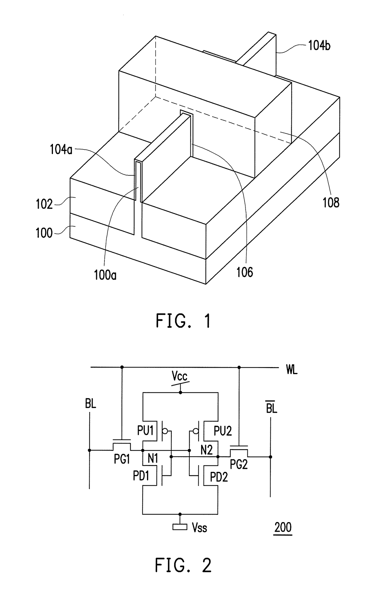
[0022]The invention is directed to an electronic circuit, which is formed from multiple fin FETs, such as a static random access memory (SRAM) formed from fin FETs. Here, the electronic device of fin FET SRAM is just an example and is not for limiting various applications of present invention.

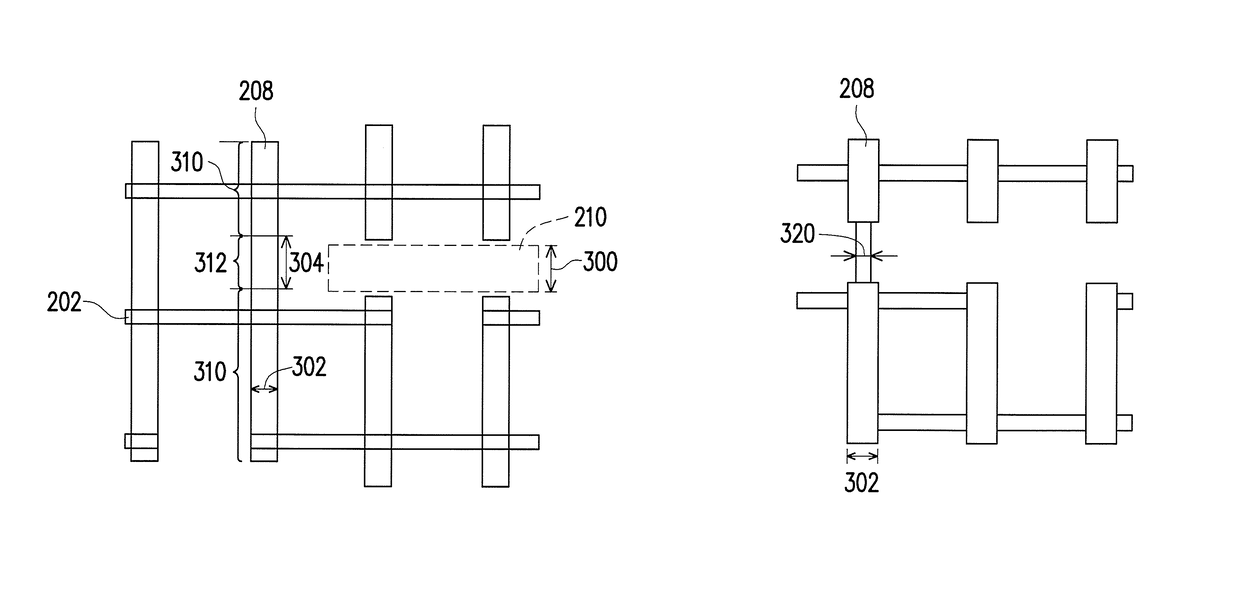
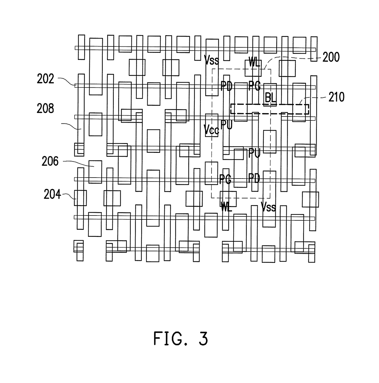
[0023]To reduce the size of FET, the fin FET has been proposed to significantly reduce a FET size. The electronic circuit then usually made from multiple fin FETs, which in view of locations can be treated as a fin FET array. The circuit has multiple fin lines on a substrate and multiple gate lines with a first line width crossing over the fin lines. The gate lines are parallel and have a plurality of discontinu...


PUM


Abstract

An electronic circuit includes a plurality of fin lines on a substrate and a plurality of gate lines with a first line width, crossing over the fin lines. The gate lines are parallel and have a plurality of discontinuous regions forming as a plurality of slots. A region of any one of the gate lines adjacent to an unbalance of the slots has a second line width smaller than the first line width.

Description

BACKGROUND OF THE INVENTION[0001]1. Field of the Invention[0002]The present invention generally relates to a semiconductor device, in particular, to an electronic circuit of fin field effect transistor (FET) and method for fabricating the electronic circuit of fin FET.[0003]2. Description of Related Art[0004]As the request to reduce the size of electronic device and increase the operation speed of electronic device, the size of the semiconductor device such as FET needs to be accordingly reduced. When size of the FET is greatly reduced, the conventional FET with polysilicon gate cannot be adapted well. So, the structure of FET in 2D structure is no longer suitable for use.[0005]In the technologies under development, a type of fin FET has been proposed. The fin FET is in 3D structure, in which the source / drain region has been raised up from the substrate, like a fin in structure. The gate can be fondled as a gate line, crossing over the fin to serve as the gate structure for each FET...

Claims


Application Information

Patent Timeline
Patent Type & Authority Patents(United States)
IPC IPC(8): H01L21/82H01L29/49H01L29/06H01L21/8234H01L27/11H01L27/088
CPCH01L21/823456H01L27/1104H01L27/0886H01L29/4916H01L29/0649H01L21/823468H01L21/823431H01L27/0207H01L21/823437H01L28/00H10B10/12
Inventor WANG, JUN-JIEWANG, YU-LINHUNG, CHING-WENLIOU, EN-CHIUANHUANG, CHIH-SEN
Owner UNITED MICROELECTRONICS CORP
Why Eureka
Try Eureka