Methods for fabricating a semiconductor device

a semiconductor and device technology, applied in the direction of semiconductor devices, electrical devices, transistors, etc., can solve the problems of increasing bridge defects between the contact and an adjacent pattern, or the gap between the contact and an adjacent active region increases

Active Publication Date: 2014-06-05
SAMSUNG ELECTRONICS CO LTD
View PDF1 Cites 7 Cited by
  • Summary
  • Abstract
  • Description
  • Claims
  • Application Information

AI Technical Summary

Benefits of technology

[0011]In example embodiments, a line width of the wiring structure may be smaller than a minimum width of the opening portion of a portion exposing the first contact forming region.

Problems solved by technology

In addition, bridge defects between the contact and an adjacent pattern or bridge defects between the contact and an adjacent active region are increasing.

Method used


Image

  • Methods for fabricating a semiconductor device
  • Methods for fabricating a semiconductor device
  • Methods for fabricating a semiconductor device

Examples


example embodiment 1

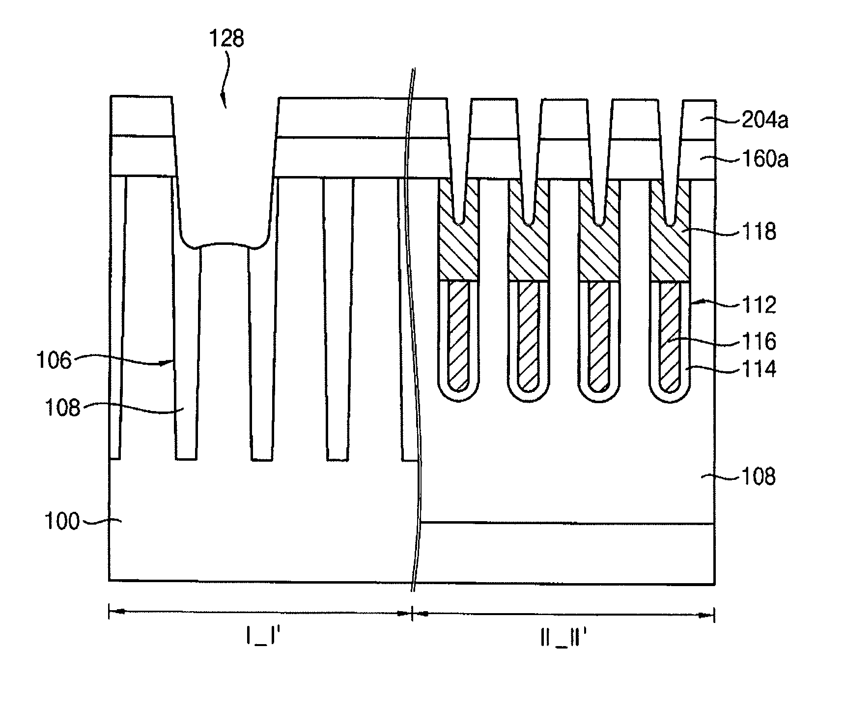
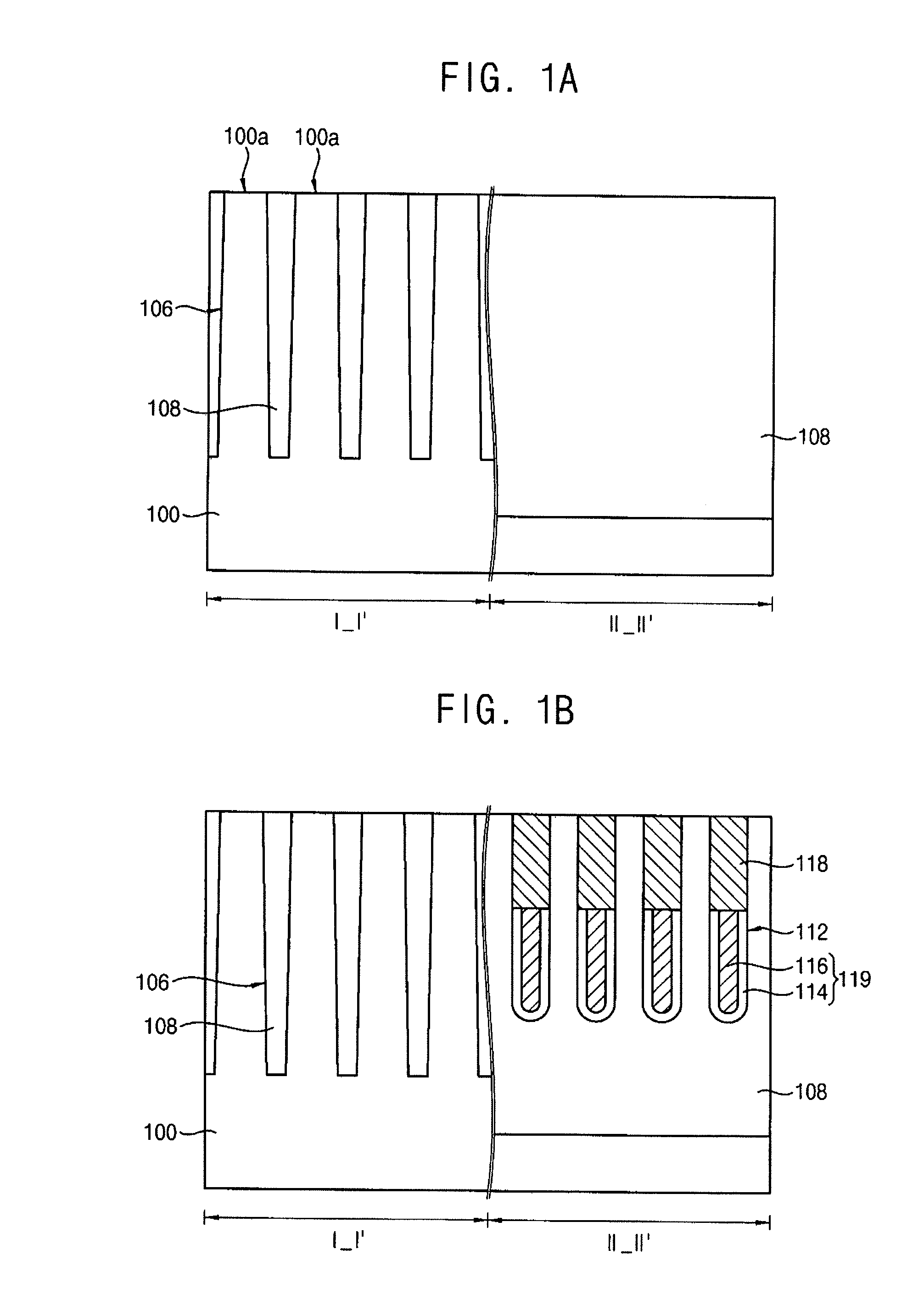
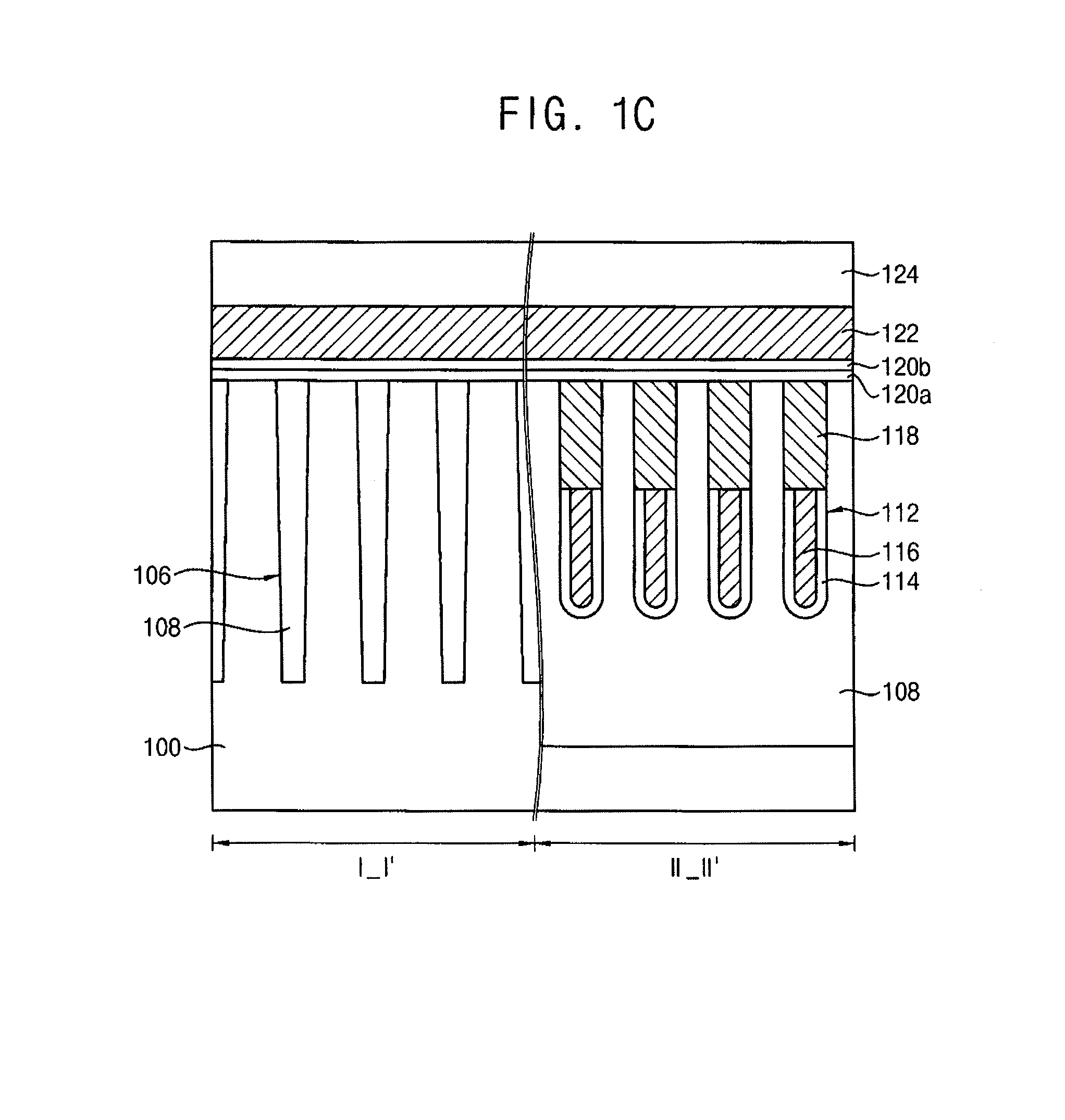
[0043]FIGS. 1A to 1J illustrate cross-sectional views of stages in a method for fabricating a semiconductor device in accordance with an exemplary embodiment. FIGS. 2A to 2G are plan views corresponding to respective cross-sectional views.

[0044]In FIGS. 1A to 1J, the left-side cross-sectional views are taken along a line I-I′ in FIG. 2A, and the right-side cross-sectional views are taken along a line II-II′ in FIG. 2A. Hereinafter, the longitudinal direction of active regions may be called as a first direction, the extended direction of buried gate structures may be called as a second direction, and a perpendicular direction to the second direction may be called as a third direction.

[0045]Referring to FIGS. 1A and 2A, a hard mask pattern (not illustrated) for forming device isolating trenches may be formed in a substrate 100 including single crystalline silicon. The hard mask pattern may include silicon nitride.

[0046]The substrate 100 may be anisotropically etched by using the hard ...

example embodiment 2

[0084]FIGS. 3A to 3F illustrate cross-sectional views of stages in a method for fabricating a semiconductor device in accordance with an exemplary embodiment.

[0085]First, the structure illustrated in FIG. 1B may be formed on a substrate by conducting the processes explained referring to FIGS. 1A and 1B.

[0086]Referring to FIG. 3A, an insulating interlayer 160 may be formed on the substrate 100 including a buried gate electrode. The insulating interlayer 160 may include, e.g., silicon oxide.

[0087]Referring to FIG. 3B, a photoresist layer may be formed on the insulating interlayer 160. The photoresist layer may be patterned through a photo process to form the photoresist patterns 126. The photoresist patterns 126 may be formed so as to have an isolated shape defining portions of the second and third contact forming regions 110b and 110c (see FIG. 2) and the adjacent upper portion of the device isolating layer pattern 108. The shape of the photoresist pattern 126 may be the same as expl...

example embodiment 3

[0097]FIGS. 4A to 4G illustrate cross-sectional views of stages in a method for fabricating a semiconductor device in accordance with an exemplary embodiment. FIG. 5 is a plan view corresponding to the cross-sectional view in FIG. 4B.

[0098]First, the same processes explained referring to FIGS. 1A to 1C may be conducted. Then, a structure including the pad insulating layer, the etch stopping layer, the first conductive layer, and the sacrificial layer stacked on the substrate including the buried gate electrode, as illustrated in FIG. 1C, may be formed.

[0099]Referring to FIG. 4A, a first mask layer 204 may be formed on the sacrificial layer 124. The first mask layer 204 may include an amorphous carbon layer (ALC).

[0100]A first anti reflecting layer 206 may be formed on the first mask layer 204. The first anti reflecting layer 206 may include, e.g., silicon oxynitride. The first anti reflecting layer 206 may be provided as an adhesive layer for improving the adhesive properties of an ...


PUM


Abstract

A method for fabricating a semiconductor device includes forming a device isolation layer pattern on a substrate to form an active region, the active region including a first contact forming region at a center p of the active region and second and third contact forming regions at edges of the active region, forming an insulating layer and a first conductive layer on the substrate, forming a mask pattern having an isolated shape on the first conductive layer, etching the first conductive layer and the insulating layer to expose the active region of the first contact forming region by using the mask pattern, to form an opening portion between pillar structures, forming a second conductive layer in the opening, and patterning the second conductive layer and the first preliminary conductive layer pattern to form a wiring structure contacting the first contact forming region and having an extended line shape.

Description

CROSS-REFERENCE TO RELATED APPLICATION[0001]Korean Patent Application No. 10-2012-0140329, filed on Dec. 5, 2012, in the Korean Intellectual Property Office, and entitled: “Methods for Fabricating A Semiconductor Device,” is incorporated by reference herein in its entirety.BACKGROUND[0002]1. Field[0003]Example embodiments relate to methods for fabricating a semiconductor device. More particularly, example embodiments relate to methods for fabricating a highly integrated DRAM device.[0004]2. Description of the Related Art[0005]Recently, semiconductor devices including DRAM devices are highly integrated. According to the increase of an integration degree, the contacting area of a contact may be decreased and a contact resistance may be increased. In addition, bridge defects between the contact and an adjacent pattern or bridge defects between the contact and an adjacent active region are increasing.SUMMARY[0006]Example embodiments provide a method for fabricating a semiconductor devic...

Claims


Application Information

Patent Timeline
Patent Type & Authority Applications(United States)
IPC IPC(8): H01L27/108
CPCH01L27/10844H10B12/053H10B12/485H10B12/0335H10B12/482H10B99/00H10B12/00
Inventor KIM, DAE-IKRYU, HO-INSON, NAK-JINHWANG, YOO-SANG
Owner SAMSUNG ELECTRONICS CO LTD
Why Eureka
Try Eureka