
Pixel array substrate and driving method thereof

a technology of pixel array and substrate, applied in the direction of instruments, semiconductor devices, optics, etc., can solve the problems that the demand for display devices is no longer limited to favorable optical characteristics and manufacturing yield

Active Publication Date: 2020-08-27
AU OPTRONICS CORP
View PDF0 Cites 8 Cited by
  • Summary
  • Abstract
  • Description
  • Claims
  • Application Information

AI Technical Summary

Benefits of technology

The patent text describes a pixel array substrate with favorable characteristics. The substrate includes a plurality of data lines, a plurality of gate lines, and a plurality of pixels. The pixels include an active device and a pixel electrode connected to the data lines and the gate lines. The substrate also includes a plurality of transfer lines arranged in a first direction and electrically connected to the gate lines. The transfer lines have a first portion and a second portion connected to each other, and a gap exists between the pixel electrode and the transfer lines. The pixels can be divided into first and second pixels, and each pixel includes a common electrode. The substrate also includes an insulation layer with first through holes and second through holes. The driving method of the pixel array substrate includes enabling one of the gate lines connected to the first second pixel of a pixel group to have a gate-on potential in a first time interval and enabling another one of the gate lines connected to the first pixel of the pixel group to have the gate-on potential in a second time interval. The technical effects of the invention include improved pixel characteristics and more efficient driving methods for the pixel array substrate.

Problems solved by technology

With the development of display technologies, the demand for display devices is no longer limited to favorable optical characteristics, such as high resolution, high contrast, and wide viewing angles.
The transfer line, however, occupies the layout area of the display region, and the number of circuits in the display region also increases, thus affecting an aperture ratio of a pixel array substrate of the display device and the manufacturing yield.

Method used


Image

  • Pixel array substrate and driving method thereof
  • Pixel array substrate and driving method thereof
  • Pixel array substrate and driving method thereof

Examples


Embodiment Construction

[0046]Reference will now be made in detail to the present embodiments of the disclosure, examples of which are illustrated in the accompanying drawings. Wherever possible, the same reference numbers are used in the drawings and the description to refer to the same or like parts.

[0047]In the accompanying drawings, the thicknesses of layers, films, panels, regions, and the like are enlarged for clarity. Throughout the specification, same reference numerals indicate same components. It should be understood that when a component such as a layer, film, region or substrate is referred to as being “on” or “connected” to another component, it may be directly on or connected to the another component, or intervening components may also be present. In contrast, when a component is referred to as being “directly on” or “directly connected to” another component, there are no intervening assemblies present. As used herein, “connection” may refer to a physical and / or electrical connection. In addi...


PUM

PropertyMeasurementUnit
widthaaaaaaaaaa
time lengthaaaaaaaaaa
line widthaaaaaaaaaa

Abstract

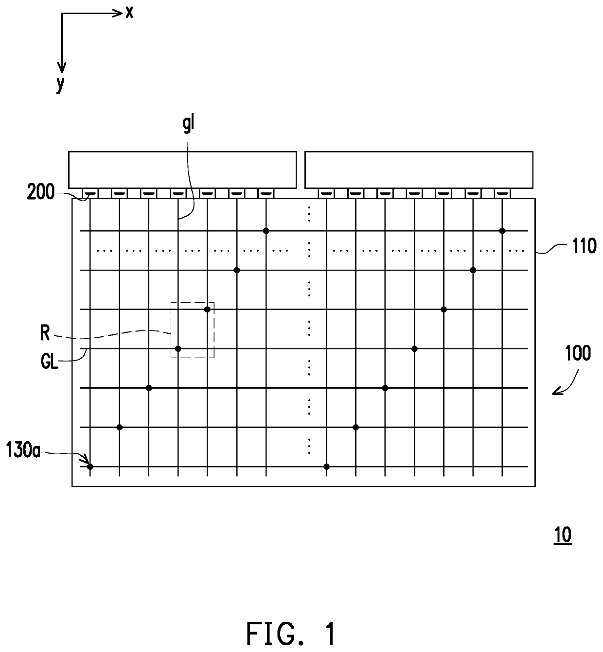
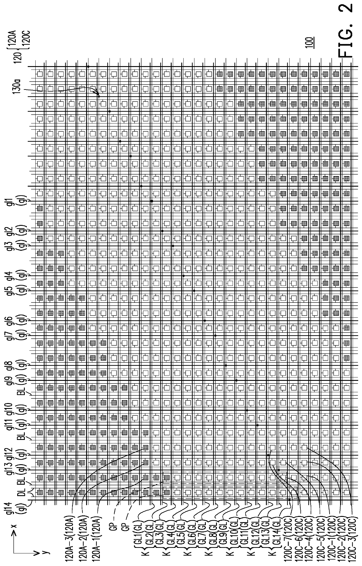
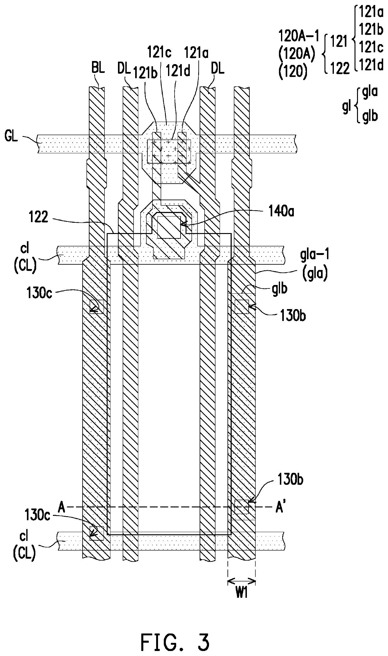
A pixel array substrate including a substrate, data lines, gate lines, pixels, and transfer lines is provided. The data lines are disposed on the substrate and arranged in a first direction. The gate lines are disposed on the substrate and arranged in a second direction interlaced with the first direction. The pixels are disposed on the substrate, each of which includes an active device electrically connected to one of the data lines and one of the gate lines and a pixel electrode electrically connected to the active device. The transfer lines are arranged in the first direction and electrically connected to the gate lines, respectively. The pixels include first pixels. In a top view of the pixel array substrate, at least one of the pixel electrodes of the first pixels is partially overlapped with one of the transfer lines. A driving method of a pixel array substrate is also provided.

Description

CROSS-REFERENCE TO RELATED APPLICATION[0001]This application claims the domestic benefit of U.S. provisional application Ser. No. 62 / 811,012, filed on Feb. 27, 2019 and the priority benefit of Taiwan patent application serial no. 108138907, filed on Oct. 28, 2019. The entirety of each of the above-mentioned patent applications is hereby incorporated by reference herein and made a part of this specification.BACKGROUNDTechnical Field[0002]The disclosure relates to a pixel array substrate and a driving method thereof.Description of Related Art[0003]With the development of display technologies, the demand for display devices is no longer limited to favorable optical characteristics, such as high resolution, high contrast, and wide viewing angles. People also expect the display devices to have elegant appearance. For instance, people expect the display devices to have narrow frames or even to be frameless.[0004]Generally speaking, the display device includes a pixel array disposed in a d...

Claims


Application Information

Patent Timeline
Patent Type & Authority Applications(United States)
IPC IPC(8): G02F1/1362
CPCG02F2201/123G02F1/136286G02F2201/121G02F1/136227G02F2001/136218H01L27/124G09G3/32G02F1/1362G02F1/136218
Inventor LEE, MIN-TSECHENG, SHENG-YENCHUNG, YUEH-HUNGLIAO, KUANG-HSIANGLEE, YANG-CHUNWANG, YAN-KAIHSU, YA-LINGCHEN, YI-RENLIN, HUNG-CHEHO, SHENG-JULIAO, CHIEN-HUANGLIAO, CHEN-HSIEN
Owner AU OPTRONICS CORP
Learn More