Atomic layer deposition method and semiconductor device formed by the same

a technology of atomic layer and semiconductor, which is applied in the direction of semiconductor devices, chemical vapor deposition coatings, coatings, etc., can solve the problems of non-uniform size distribution of atomic islands, achieve small line width, enhance charge trapping capability, and improve the density of well in the charge trapping layer

Active Publication Date: 2012-09-25
SEMICONDUCTOR MANUFACTURING INTERNATIONAL (BEIJING) CORP
View PDF10 Cites 7 Cited by
  • Summary
  • Abstract
  • Description
  • Claims
  • Application Information

AI Technical Summary

Benefits of technology

[0028]As compared with the prior art, the present invention has the following advantages:
[0030]Further, in the atomic layer deposition method, a first discrete monolayer is formed on a semiconductor substrate by controlling the feeding of the first precursor gas to the deposition chamber, for example, by reducing the flow rate of the first precursor gas and the deposition time. And also the distribution density of the first monolayer on the semiconductor substrate is adjusted by controlling the flow rate and time of the first precursor gas feeding to the deposition chamber.
[0034]The semiconductor device according to the present invention has a small line width and improves the density of well in the charge trapping layer, thus enhance the charge trapping capability. And also it may improve the insulating capacity between the discrete atomic size islands, thereby reducing lateral current leakage of the device.

Problems solved by technology

However, in the prior art, the charge trapping layer having discrete atomic islands (nano-dot) is generally formed by chemical vapor deposition or physical vapor deposition, and the size of the resulting atomic islands is in a range of 10 nm to 100 nm, and the size distribution of the atomic islands is non-uniform.

Method used


Image

  • Atomic layer deposition method and semiconductor device formed by the same
  • Atomic layer deposition method and semiconductor device formed by the same
  • Atomic layer deposition method and semiconductor device formed by the same

Examples


embodiment 1

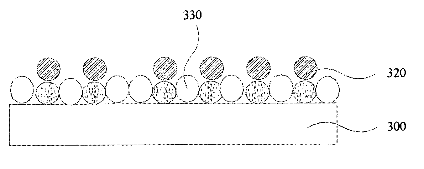
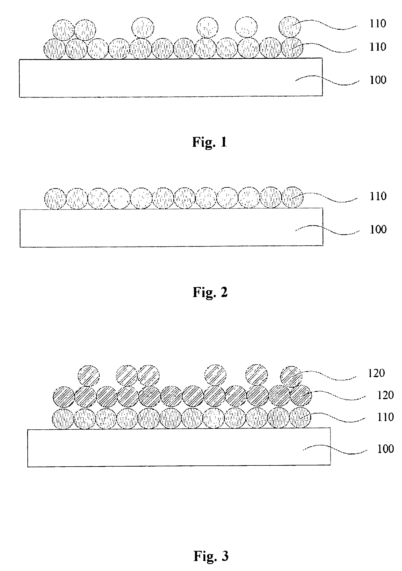
[0044]An atomic layer deposition method is provided in this embodiment. Referring to the flow diagram shown in FIG. 9, the method comprises the steps of: placing a semiconductor substrate in an atomic layer deposition chamber (step S200); feeding a first precursor gas to the semiconductor substrate within the deposition chamber to form a first discrete monolayer on the semiconductor substrate (step S201); feeding an inert purge gas to the semiconductor substrate within the chamber to remove the first precursor gas which has not formed the first discrete monolayer (step S202); feeding a second precursor gas to the chamber to react with the first precursor gas which has formed the first discrete monolayer, thereby forming a discrete atomic size islands (step S203); and feeding an inert purge gas to the chamber to remove the second precursor gas which has not reacted with the first precursor gas and byproducts produced by the reaction between the first and the second precursor gases (s...

embodiment 2

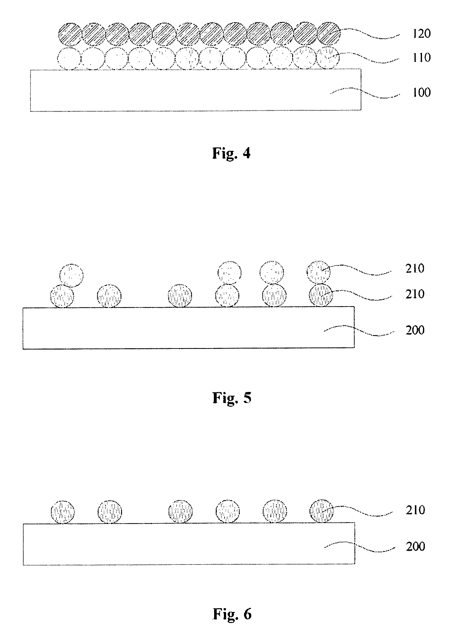
[0074]An atomic layer deposition method is provided in this embodiment. Referring to the flow diagram shown in FIG. 16, the method comprises the steps of: placing a semiconductor substrate in an atomic layer deposition chamber (step S300); feeding a first precursor gas to the semiconductor substrate within the deposition chamber to form a first discrete monolayer on the semiconductor substrate (step S301); feeding an inert purge gas to the semiconductor substrate within the chamber to remove the first precursor gas which has not formed the first discrete monolayer (step S302); feeding a second precursor gas to the chamber to react with the first precursor gas which has formed the first discrete monolayer, thereby forming a discrete atomic size islands (step S303); and feeding an inert purge gas to the chamber to remove the second precursor gas which has not reacted with the first discrete monolayer and byproducts produced by the reaction between the first and the second precursor ga...

embodiment 3

[0106]Referring to the FIG. 17, there is provided a semiconductor device in this embodiment, which comprises a semiconductor substrate 400, a three-layer stack structure of medium layer 430-charge trapping layer 440-medium layer 450 disposed on the semiconductor substrate 400, a gate 460 disposed on the three-layer stack structure, and a source 410 and a drain 420 disposed in the semiconductor substrate 400 at each side of the three-layer stack structure, wherein the charge trapping layer 440 is a dielectric layer containing the discrete atomic size islands formed by the ALD deposition method. Herein the word “containing” means that the discrete atomic size islands are embedded in the dielectric layer and covered by the dielectric layer.

[0107]The semiconductor substrate 400 can include silicon or silicon germanium (SiGe) with monocrystal or polycrystal structures, ion-doped Si or SiGe such as N-doped or P-doped Si or SiGe, compound semiconductor such as silicon carbide, indium antim...


PUM

PropertyMeasurementUnit
pressureaaaaaaaaaa
size distributionaaaaaaaaaa
temperatureaaaaaaaaaa

Abstract

Disclosed are atomic layer deposition method and a semiconductor device including the atomic layer, including the steps: placing a semiconductor substrate in an atomic layer deposition chamber; feeding a first precursor gas to the semiconductor substrate within the chamber to form a first discrete monolayer on the semiconductor substrate; feeding an inert purge gas to the semiconductor substrate within the chamber to remove the first precursor gas which has not formed the first discrete monolayer on the semiconductor substrate; feeding a second precursor gas to the chamber to react with the first precursor gas which has formed the first discrete monolayer, forming a discrete atomic size islands; and feeding an inert purge gas to the semiconductor substrate within the chamber to remove the second precursor gas which has not reacted with the first precursor gas and byproducts produced by the reaction between the first and the second precursor gases.

Description

[0001]This application claims the priority of Chinese Patent Application No. 200710042457.9, filed Jun. 22, 2007, the entire disclosure of which is incorporated herein by reference.FIELD OF THE INVENTION[0002]The present invention relates to a method for manufacturing a semiconductor device, and more particularly, to an atomic layer deposition method and a semiconductor device manufactured by the same.DESCRIPTION OF THE RELATED ART[0003]Atomic layer deposition (ALD) is originally referred to as Atomic Layer Epitaxy (ALE), and is also termed as Atomic Layer Chemical Vapor Deposition (ALCVD).[0004]Atomic layer deposition (ALD) involves the deposition of successive single layers over a semiconductor substrate within a deposition chamber typically maintained at a negative pressure (a pressure below the atmospheric pressure). An exemplary method is disclosed in the Chinese patent application No. 03818269.6, which comprises feeding a first vaporized precursor to a deposition chamber to fo...

Claims


Application Information

Patent Timeline
Patent Type & Authority Patents(United States)
IPC IPC(8): H01L21/20
CPCC23C16/04C23C16/45527H01L21/02164H01L21/0217H01L21/02178H01L21/02181H01L21/0228H01L21/28282H01L21/3141H01L21/31616H01L21/3185H01L29/40117
Inventor JI, HUACHI, MIN-HWAMIENO, FUMITAKE
Owner SEMICONDUCTOR MANUFACTURING INTERNATIONAL (BEIJING) CORP
Why Eureka
Try Eureka