Method of manufacturing a transparent substrate

a technology of transparent substrates and manufacturing methods, applied in the direction of conductive layers on insulating supports, magnetic circuits characterised by magnetic materials, instruments, etc., can solve the problems of increased defect rate, difficult to implement such a fine line width, and deterioration in display quality, so as to improve transparency and improve transparency. , the effect of superior transparency

Active Publication Date: 2017-09-26
LG CHEM LTD
View PDF15 Cites 0 Cited by
  • Summary
  • Abstract
  • Description
  • Claims
  • Application Information

AI Technical Summary

Benefits of technology

[0025]In a manufacturing method of a transparent substrate according to exemplary embodiments of the present disclosure, a significantly fine metal line having a line width of 3 μm or less may be formed and accordingly, a deterioration in transparency due to the reflection of the fine metal line may be significantly reduced, such that a transparent substrate having superior transparency may be manufactured. Therefore, the transparent substrate manufactured according to exemplary embodiments of the present disclosure may be usefully employed in the field of displays such as touch panels or transparent organic light emitting diodes (OLEDs).
[0026]Further, according to the manufacturing method of the transparent substrate, since a transparent substrate including a conductive layer may be manufactured through a consecutive process such as a roll-to-roll process, productivity thereof may be excellent and manufacturing costs required therefor may be relatively low. Moreover, the manufacturing method may have environmentally friendly characteristics capable of significantly decreasing the generation of chemical waste products through physical metal removal.

Problems solved by technology

Meanwhile, in conductive substrates used in display devices or touch panels, in a case in which a line width of a conductive pattern exceeds 3 μm, the conductive pattern may be easily visually discernible from the outside of the substrate due to a difference in reflectance between a conductive pattern layer and the substrate, thereby leading to a deterioration in display quality.
However, it may be difficult to implement such a fine line width using a manufacturing method of a conductive substrate according to the related art.
Here, in a case in which conductivity of the resin is significantly low as compared to that of a solid metal and a process rate thereof is increased, a non-filled region in the groove may be easily generated, thereby leading to an increase in a defect rate.
In addition, in order to implement a fine line width of 3 μm or less, a conductive material filled in a groove needs to have a significantly fine nano-size, but it may be practically unfeasible to reduce a size of the conductive material in such a manner.
Meanwhile, in the case of a method of compressing metal particles or metal oxide particles by applying heat and / or pressure thereto, pattern deformation may easily occur due to heat and / or pressure to deteriorate the degree of precision, thereby causing limitations in the formation of fine patterns.
However, since it may be practically difficult to implement ink droplets sizes in such a manner, the scheme of performing printing using a conductive ink may be inappropriate for forming patterns having a line width of 3 μm or less.
In addition, in the case of the plating scheme, since it may be difficult to selectively perform plating only on a groove, a metal layer formed on a region other than the groove needs to be removed through a polishing operation using polishing particles after the plating.
However, in this case, since it may be difficult to apply a consecutive process such as a roll-to-roll process thereto, a relatively long manufacturing time may be required, and relatively cumbersome processes may be caused.

Method used


Image

  • Method of manufacturing a transparent substrate
  • Method of manufacturing a transparent substrate
  • Method of manufacturing a transparent substrate

Examples


experimental example 1

Whether or not Short-circuits Occur

[0102]The transparent substrates manufactured according to Inventive Example and Comparative Examples 1 and 2 were imaged by using a scanning electron microscope (SEM) to observe whether or not short-circuits occurred in the conductive layers thereof. FIGS. 6 to 8 are images obtained by imaging the transparent substrates manufactured according to Inventive Example and Comparative Examples 1 and 2. FIGS. 6(A) and 6(B) are images obtained by imaging the substrate according to Inventive Example, while changing an angle and a magnification of the microscope. FIG. 7 is an image obtained by imaging the transparent substrate according to Comparative Example 1. FIG. 8 is an image obtained by imaging the transparent substrate according to Comparative Example 2. Referring to FIG. 6, it could be confirmed that in the case of the substrate manufactured according to the exemplary embodiment of the present disclosure, the conductive layer present within the groo...

experimental example 2

Measurement of Conductivity

[0103]Resistance values of the transparent substrates manufactured by Inventive Example and Comparative Examples 1 and 2 were measured by using a Fluke 117 Multi-meter manufactured by the Fluke Company. Measured results are described in the following Table 1.

[0104]

TABLE 1ClassificationResistance valueInventive~17.2 Ω / □ExampleComparativenon-conductiveExample 1Comparativenon-conductiveExample 2

Reference Numerals

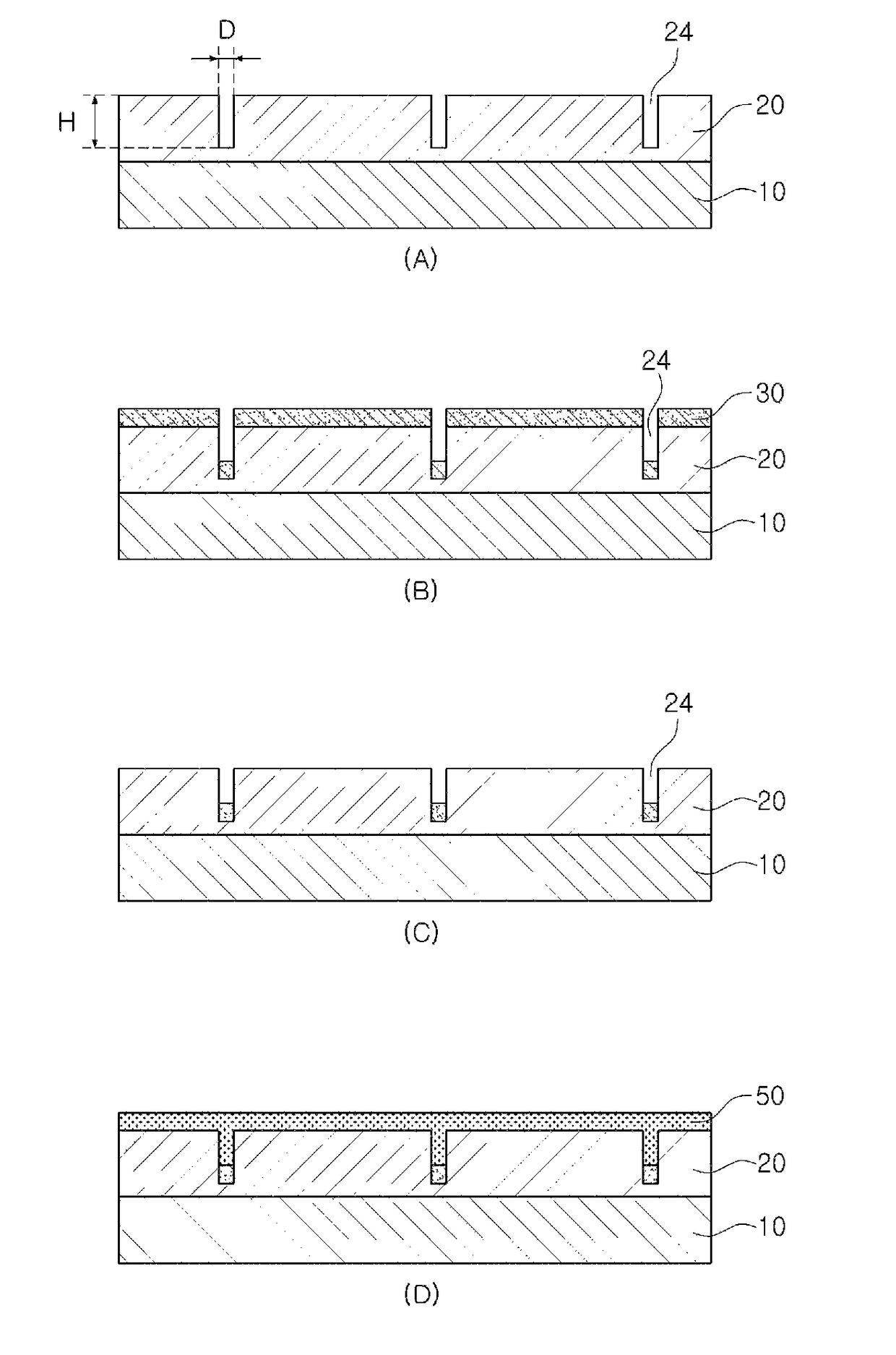
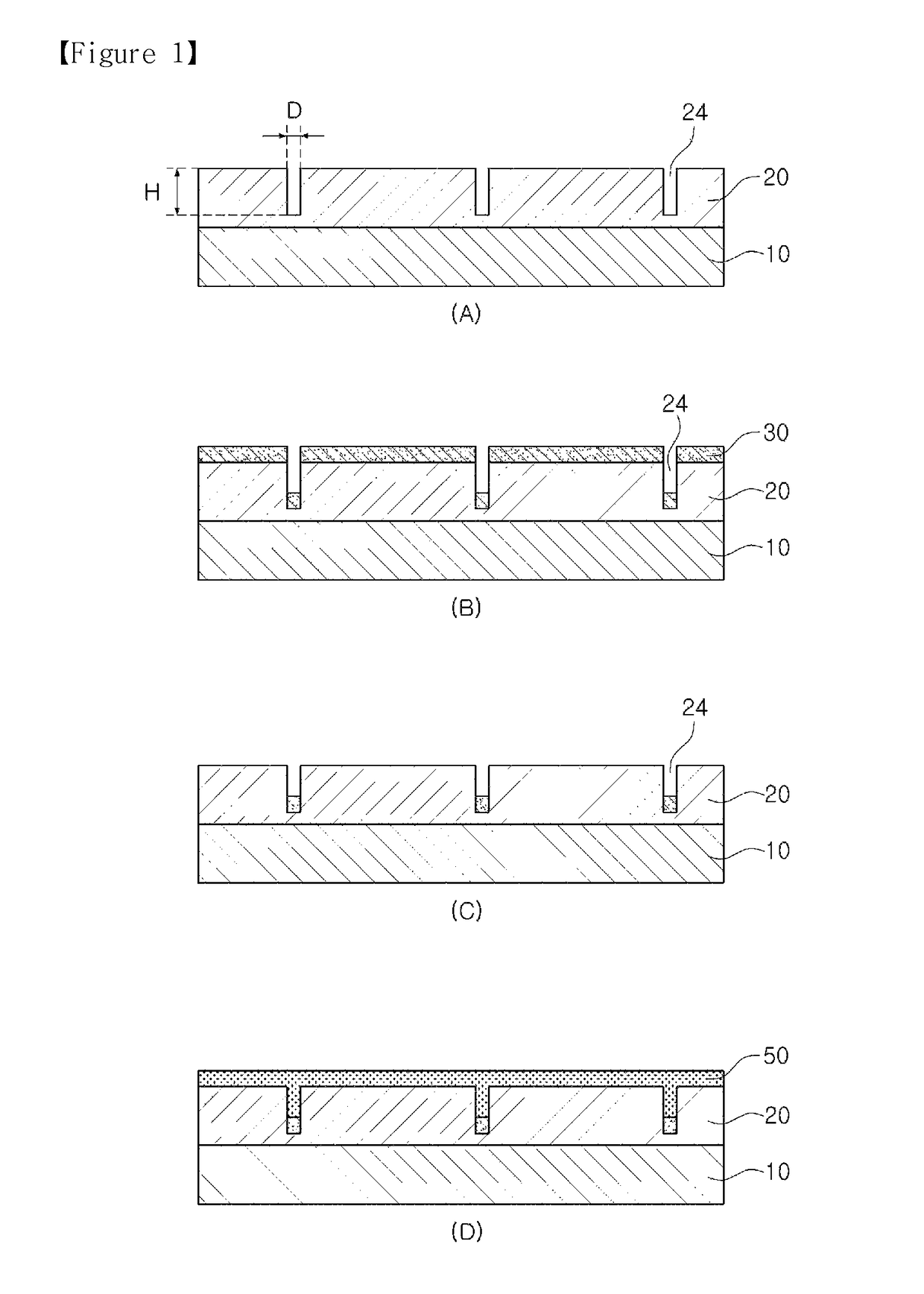
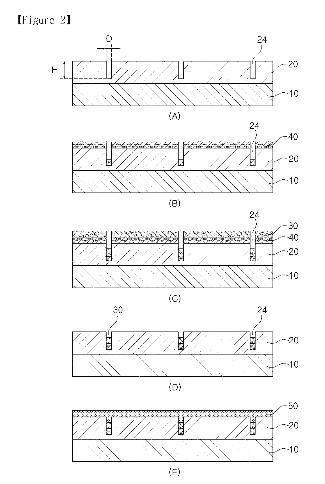
[0105]10: Transparent Substrate[0106]20: Resin Pattern Layer[0107]24: Grooves[0108]30: Conductive Layer[0109]40: Adhesion Controlling Layer[0110]50: Planarized Layer[0111]60: Fine Particles


PUM

PropertyMeasurementUnit
widthaaaaaaaaaa
angle of inclinationaaaaaaaaaa
deposition angleaaaaaaaaaa

Abstract

The present disclosure relates to a transparent substrate including: a resin pattern layer including a plurality of grooves respectively including side surfaces and a bottom surface; and, a conductive layer formed within the grooves, wherein a line width of the conductive layer is 0.1 μm to 3 μm and an average height of the conductive layer is 5% to 50% of a maximum depth of each of the grooves, and a manufacturing method thereof, such that simplicity in a manufacturing process and a consecutive process are enabled, manufacturing costs are inexpensive, and a transparent substrate having superior electrical conductivity and transparency characteristics is manufactured.

Description

[0001]This application is a 35 USC §371 National Stage entry of International Application No. PCT / KR2014 / 001906, filed Mar. 7, 2014, and claims priority to Korean Application Nos. 10-2013-0024661, filed Mar. 7, 2013 and 10-2014-0027237, filed Mar. 7, 2014, all of which are hereby incorporated by reference in their entirety.TECHNICAL FIELD[0002]The present disclosure relates to a transparent substrate and a manufacturing method thereof, and more particularly, to a transparent substrate including a fine metal line having a line width of 3 μm or less and providing superior electrical conductivity and transparency characteristics, and a manufacturing method thereof.BACKGROUND ART[0003]Conductive substrates having fine conductive patterns formed on a polymer film or a glass substrate have been used in various fields of applications such as electromagnetic wave-shielding filters, heating wire glass, touch panels, liquid crystal displays and the like, within various fields of application. ...

Claims


Application Information

Patent Timeline
Patent Type & Authority Patents(United States)
IPC IPC(8): H02K1/02H05K1/02H05K3/04H05B3/12H05B3/84H05K1/03H05K1/09H05K3/00H05K3/14H05K3/38G03F7/00
CPCH05K1/0296H05B3/12H05B3/84H05K1/0274H05K1/0313H05K1/09H05K3/0023H05K3/0044H05K3/04H05K3/045H05K3/146H05K3/38G03F7/00H05B2203/017H05K2201/0108H05K2201/0129H05K2201/0317H05K2201/09036H05K2203/0108H01B5/14
Inventor BAE, SUNG-HAKHAN, SANG-CHOLLKIM, BYONG-MOOK
Owner LG CHEM LTD
Why Eureka
Try Eureka