Device for electrically testing the interconnections of a microelectronic device

a microelectronic device and interconnection technology, applied in the direction of base element modification, semiconductor/solid-state device testing/measurement, instruments, etc., can solve the problem of electrical testing of devices formed by stacked wafers, and achieve the effect of restricting the overall size and simple logic functions

Active Publication Date: 2017-10-10
COMMISSARIAT A LENERGIE ATOMIQUE ET AUX ENERGIES ALTERNATIVES
View PDF16 Cites 0 Cited by
  • Summary
  • Abstract
  • Description
  • Claims
  • Application Information

AI Technical Summary

Benefits of technology

[0019]With such a device, an electrical test can be simultaneously carried out on several of said interconnection elements without necessarily having to test simultaneously all the interconnection elements of the microelectronic device.
[0021]The removability of said connection means provided on the first face enables in particular the overall size of the device to be reduced once the test is carried out, and the connection between said interconnection elements to be suppressed when the microelectronic device is no longer subjected to a test.
[0024]According to a first possibility of implementation, this testing circuit can comprise at least one logic gate, in particular means forming an OR logic gate or an AND logic gate, connected to interconnection elements of said first plurality of interconnection elements. It is thus possible to implement a testing device with simple logic functions and having a restricted overall size.

Problems solved by technology

The electrical testing of devices formed by stacked wafers has several problems.
The problem arises to make an electrical test of a plurality of interconnection elements passing through a substrate without necessarily having to test all the interconnection elements passing through this substrate.

Method used


Image

  • Device for electrically testing the interconnections of a microelectronic device
  • Device for electrically testing the interconnections of a microelectronic device
  • Device for electrically testing the interconnections of a microelectronic device

Examples


Embodiment Construction

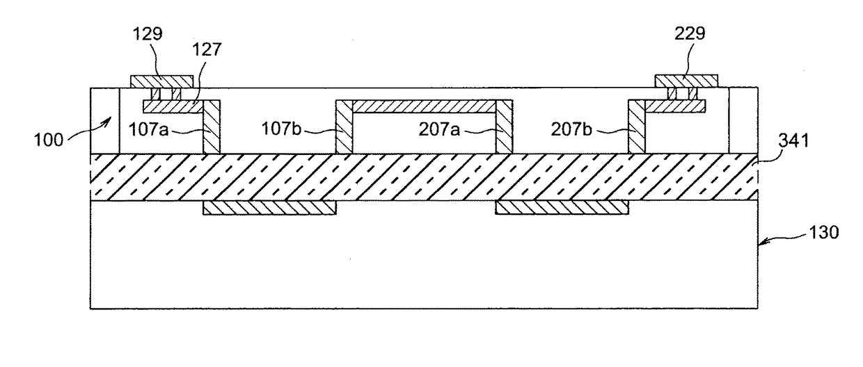
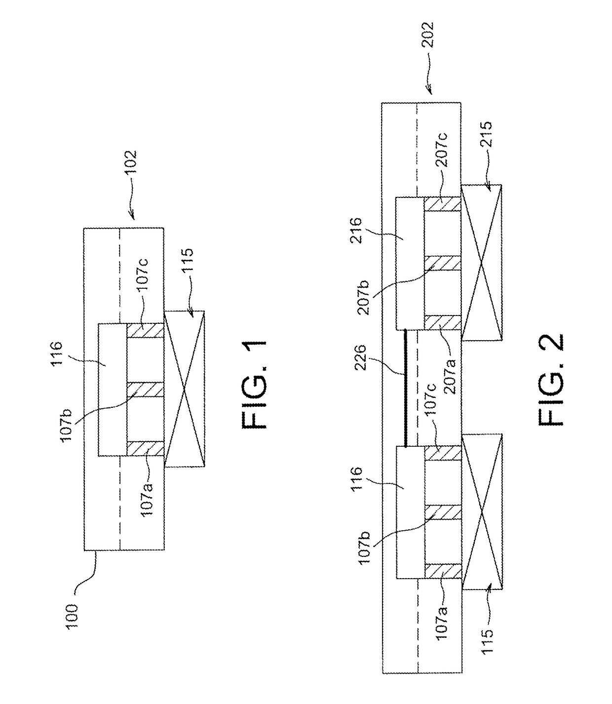
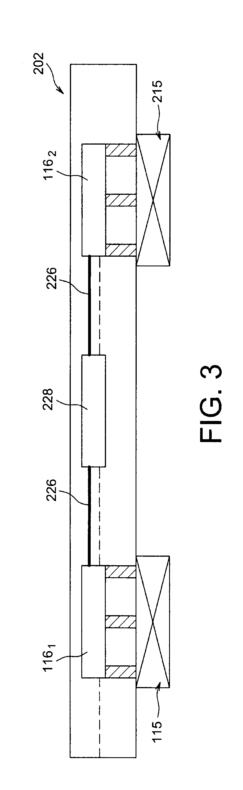
[0048]A first example of device for implementing electrical test(s) on one or several TSV type interconnection elements provided in a chip, is given in FIG. 1.

[0049]In this example, a chip 102 includes TSV type interconnection elements 107a, 107b, 107c passing at least partly through the thickness of a carrier. This carrier can in particular be a semi-conductor substrate, on which or from which the chip 102 is formed.

[0050]These connection elements 107a, 107b, 107c include a conductive portion or conductive area passing through the thickness of the semi-conductor substrate.

[0051]This conductive portion can for example be in the form of a post, possibly in contact with one or more so-called “redistribution” conductive layers and / or with one or more conductive beads. The conductive portion can be metallic and for example based on copper or aluminium, or comprise a silver, gold, titanium or tin based conductive material.

[0052]The connection elements 107a, 107b, 107c can be each surroun...


PUM


Abstract

A simultaneous electrical testing device for TSV interconnection elements passing through a substrate and including one end connected to an integrated testing circuit and another end to a removable connection mechanism assembled to the substrate through an anisotropic conductive glue.

Description

TECHNICAL FIELD[0001]The present application relates to the field of devices for electrically testing interconnection elements in a microelectronic device enabling the electrical continuity and / or electrical characteristics of interconnection elements passing through a carrier to be checked, in particular of vertical or TSV type interconnection elements, as well as a method for electrically testing interconnection elements.PRIOR ART[0002]In order to achieve a high integration density, it is known to make microelectronic devices formed by stacks of carriers or wafers, each comprising one or more chips which are thus distributed on several levels. To make interconnections in such a type of device, connection elements of the type commonly called “TSV” (“Through Silicon Via”) are generally provided. These connection elements pass at least partly through the thickness of a substrate and possibly one or more wafers and carriers stacked above this substrate.[0003]An interconnection element...

Claims


Application Information

Patent Timeline
Patent Type & Authority Patents(United States)
IPC IPC(8): G01R31/28G01R1/20H01L21/66
CPCG01R31/2853G01R1/20H01L22/14H01L22/34H01L2924/0002H01L2924/00
Inventor BEN JAMAA, HAYKEL
Owner COMMISSARIAT A LENERGIE ATOMIQUE ET AUX ENERGIES ALTERNATIVES
Why Eureka
Try Eureka