
Display device and drive method therefor

a technology of display device and drive method, which is applied in the direction of static indicating device, instruments, etc., can solve the problems of reducing display quality, difficulty in increasing size and definition, and affecting the quality of display, so as to reduce the amount of measurement time, the effect of sufficient length of monitoring period and sufficient amount of tim

Active Publication Date: 2017-12-05
SHARP KK
View PDF14 Cites 2 Cited by
  • Summary
  • Abstract
  • Description
  • Claims
  • Application Information

AI Technical Summary

Benefits of technology

This patent describes a display device that can detect the characteristics of individual pixel circuits and adjust the video signal to compensate for any degradation of the drive transistor or electro-optical element. This allows for a longer monitoring period and ensures sufficient time for the detection of the characteristics of both components. Additionally, this technology can reduce measurement time and cause the electro-optical element to emit light at the desired brightness while detecting its characteristics. Furthermore, this approach can detect multiple properties of the electro-optical element and compensate for degradation more efficiently.

Problems solved by technology

An organic EL display device that adopts the passive matrix system has a simple structure but is difficult to increase in size and definition.
In a thin-film transistor, however, variations in threshold voltage are likely to occur.
Variations in threshold voltage occurring in a drive transistor provided in a display unit cause variations in brightness, resulting in a reduction in display quality.
However, the current efficiency of the organic EL element decreases with time.
This leads to burn-in.

Method used


Image

  • Display device and drive method therefor
  • Display device and drive method therefor
  • Display device and drive method therefor

Examples


first embodiment

1. First Embodiment

[0171]1.1 Overall Configuration

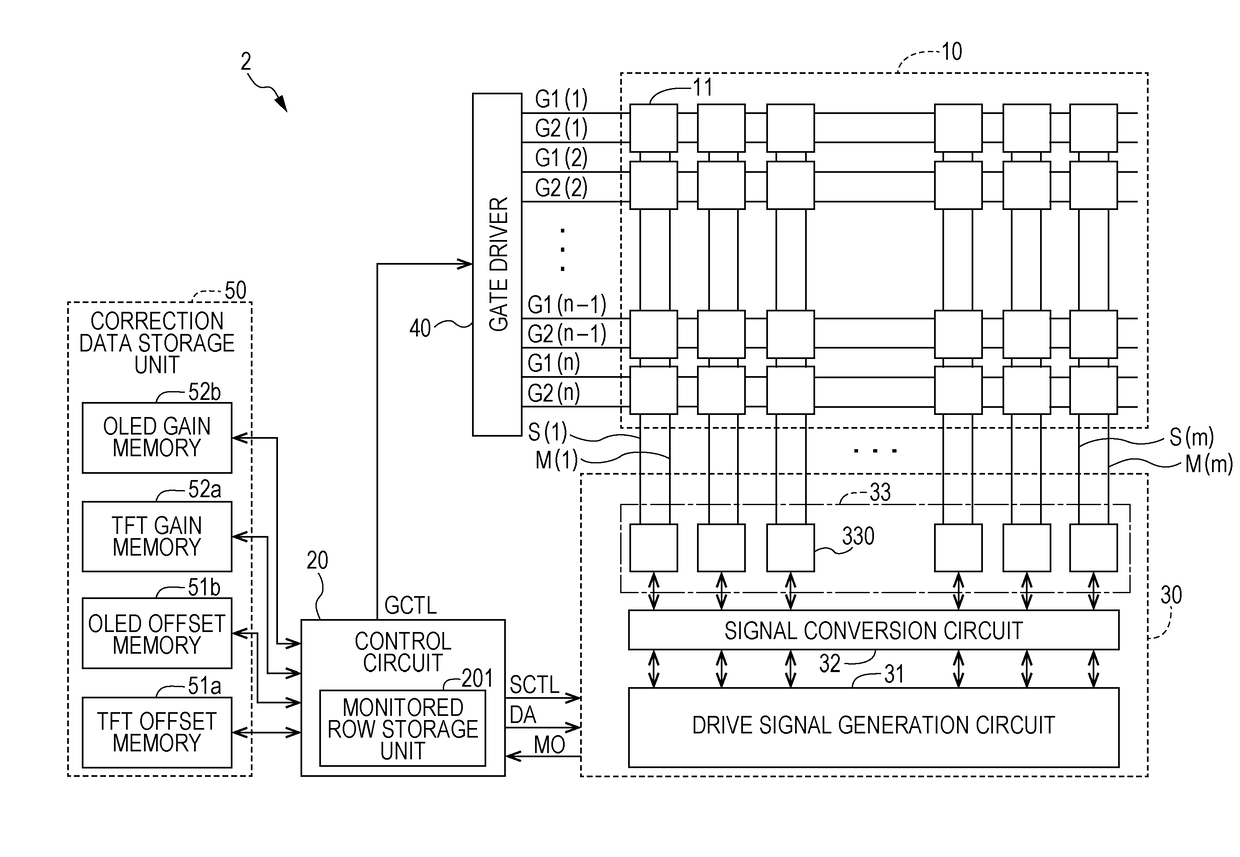
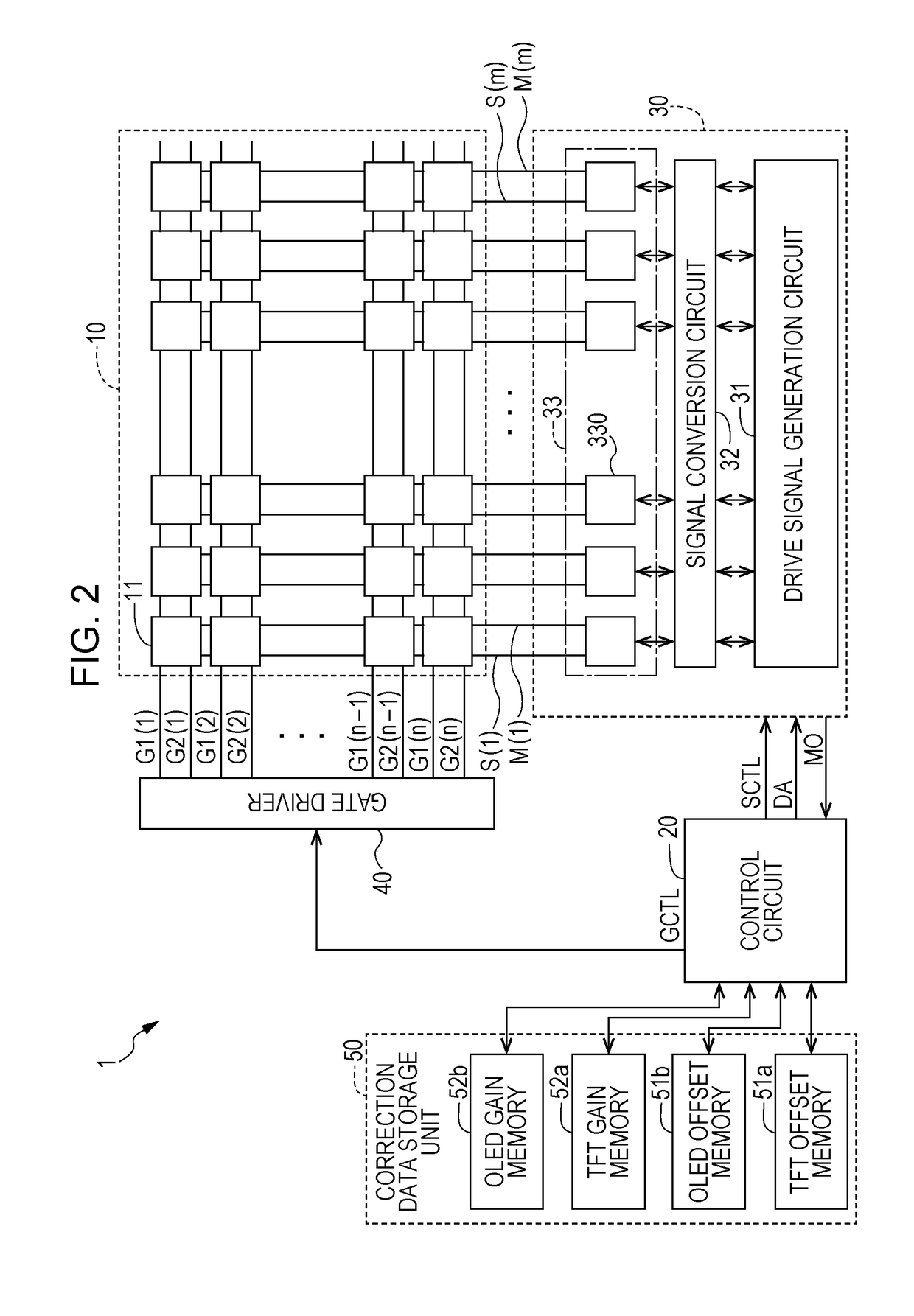
[0172]FIG. 2 is a block diagram illustrating the overall configuration of an active-matrix organic EL display device 1 according to a first embodiment of the present invention. The organic EL display device 1 includes a display unit 10, a control circuit 20, a source driver (data line driving circuit) 30, a gate driver (scanning line driving circuit) 40, and a correction data storage unit 50. In this embodiment, the source driver 30 and the gate driver 40 implement a pixel circuit driving unit. Either or both of the source driver 30 and the gate driver 40 may be configured to be integrated with the display unit 10 into a single unit.

[0173]The display unit 10 has disposed thereon m data lines S(1) to S(m) and n scanning lines G1(1) to G1(n) intersecting the m data lines S(1) to S(m). In the following, a direction in which data lines extend is referred to as a Y direction, and a direction in which scanning lines extend is referred to a...


PUM


Abstract

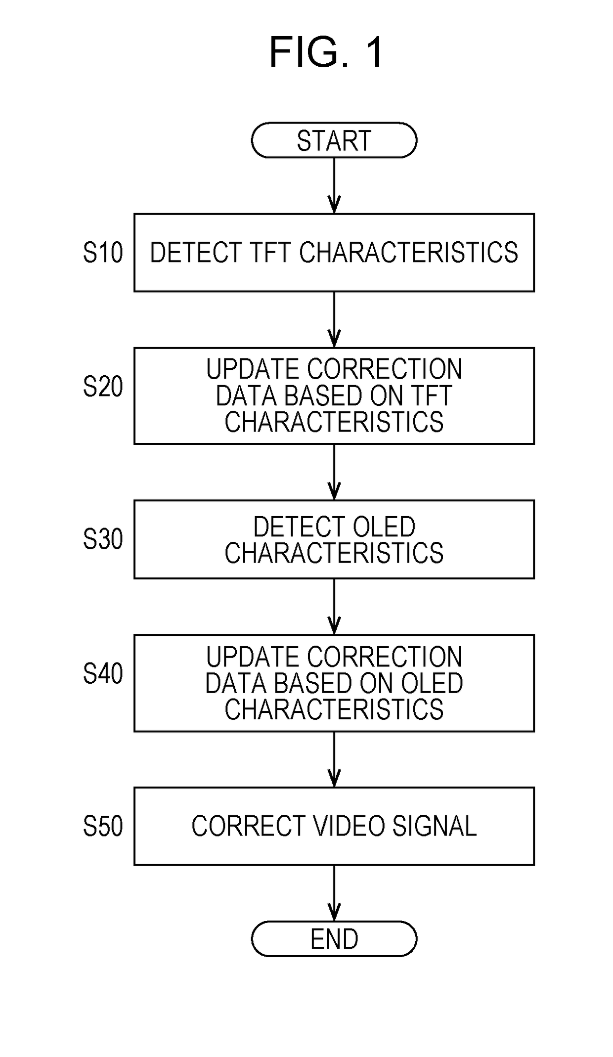
A monitor line electrically connectable with sources of drive transistors and positive electrodes of electro-optical elements is provided. A drive method includes a step of detecting the characteristics of a drive transistor, a step of detecting the characteristics of an electro-optical element, a step of storing characteristics data obtained on the basis of a result of the detection of the characteristics, as correction data for correcting a video signal, and a step of correcting the video signal on the basis of the correction data. Here, the length of a selection period is set to be equal for a monitored row and an unmonitored row. In addition, a potential given to the monitor line for the detection of the characteristics of the drive transistors and a potential given to the monitor line for the detection of the characteristics of the electro-optical elements are made different.

Description

TECHNICAL FIELD[0001]The present disclosure relates to display devices and drive methods therefor, and more specifically to a display device provided with pixel circuits each including an electro-optical element such as an organic EL (Electro Luminescence) element, and to a drive method for the display device.BACKGROUND ART[0002]In the related art, examples of a display element provided in a display device include an electro-optical element whose brightness is controlled with applied voltage, and an electro-optical element whose brightness is controlled with current. Typical examples of the electro-optical element whose brightness is controlled with applied voltage include a liquid crystal display element. On the other hand, typical examples of the electro-optical element whose brightness is controlled with current include an organic EL element. The organic EL element is also called an OLED (Organic Light-Emitting Diode). An organic EL display device including an organic EL element,...

Claims


Application Information

Patent Timeline
Patent Type & Authority Patents(United States)
IPC IPC(8): G09G3/30G09G3/3208G09G3/3233G09G3/3291
CPCG09G3/3208G09G3/3233G09G3/3291G09G2300/043G09G2300/0842G09G2320/0666G09G2310/06G09G2320/0295G09G2320/043G09G2320/0626G09G2310/0218
Inventor KISHI, NORITAKA
Owner SHARP KK
Learn More