Deposition method for planar surfaces

a planar surface and surface technology, applied in the field of manufacturing and processing of semiconductor wafers, can solve the problems of over-etching of features below the deposited material around the edges, focusing errors tor which corrections, and the shape of the ground will adversely affect subsequent processing steps, so as to reduce or eliminate the long-range distortion of deposition induced lithography, planarization and other process steps.

Active Publication Date: 2017-12-05
WESTERN DIGITAL TECH INC
View PDF7 Cites 0 Cited by
  • Summary
  • Abstract
  • Description
  • Claims
  • Application Information

AI Technical Summary

Benefits of technology

[0008]The present disclosure generally relates to a method for producing a substantially planar surface for semiconductor processing to improve lithography, planarization, and other process steps that benefit from a flat substrate. The method includes depositing a first alloy to form a first layer on a substrate. The first layer has a center high deposition, meaning the height in the center of the substrate is higher than the height at the edges of the substrate. The method further includes depositing a second alloy on the first layer to form a second layer. The first alloy has a different composition than the second alloy. In such a method the net deposition is substantially planar reducing or eliminating deposition induced long-range distortions that might occur across a substrate.

Problems solved by technology

This mound shape will adversely affect subsequent processing steps such as etching, Chemical Mechanical Polishing, (CMP), lithographic exposures, to name a few.
For example, when etching, the material deposited on the surface will be removed around the edges before it is removed in the center and, as a result, continuing the etch to clear the center area will cause over-etching of the features below the deposited material around the edges.
In lithographic exposures, a domed wafer might be closer to the exposure source at the edges than at the center of the wafer resulting in focusing errors tor which corrections would have to be made.

Method used


Image

  • Deposition method for planar surfaces
  • Deposition method for planar surfaces
  • Deposition method for planar surfaces

Examples


Embodiment Construction

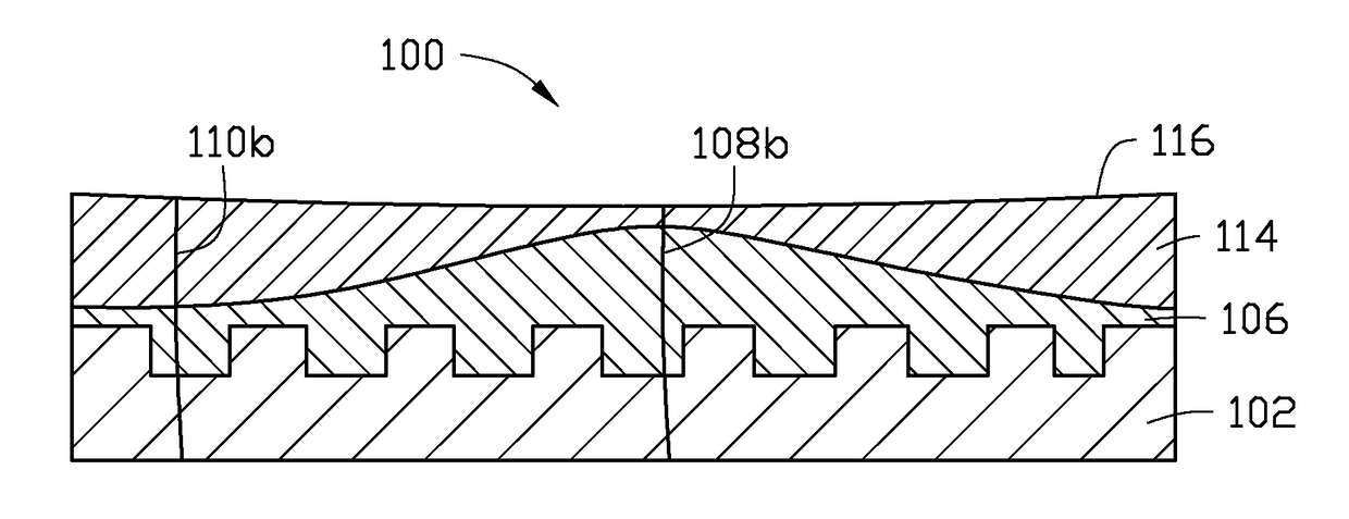
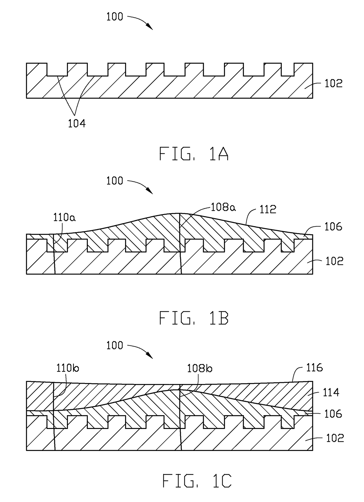
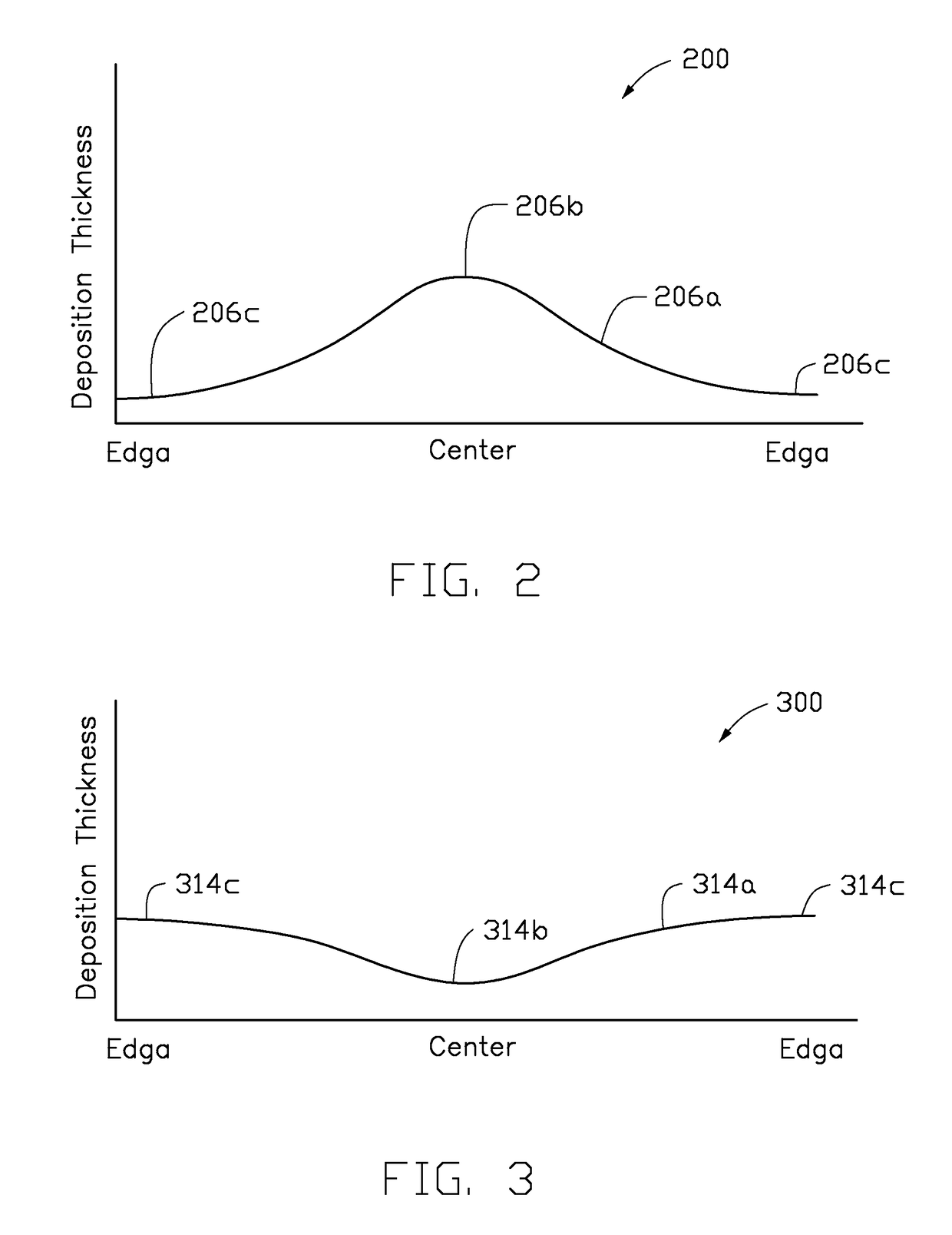
[0018]In the following, reference is made to embodiments of the disclosure. However, it should be understood that the disclosure is not limited to specific described embodiments. Instead, any combination of the following features and elements, whether related to different embodiments or not, is contemplated to implement and practice the disclosure. Furthermore, although embodiments of the disclosure may achieve advantages over other possible solutions and / or over the prior art, whether or not a particular advantage is achieved by a given embodiment is not limiting of the disclosure. Thus, the following aspects, features, embodiments and advantages are merely illustrative and are not considered elements or limitations of the appended claims except where explicitly recited in a claim(s). Likewise, reference to “the disclosure” shall not be construed as a generalization of any inventive subject matter disclosed herein and shall not be considered to be an element or limitation of the ap...


PUM

PropertyMeasurementUnit
aspect ratioaaaaaaaaaa
thicknessaaaaaaaaaa
heightaaaaaaaaaa

Abstract

A method for producing a substantially planar surface for semiconductor processing to improve lithography, planarization, and other process steps that benefit from a flat substrate. The method includes depositing a first alloy to form a first layer on a substrate. The first layer has a center high deposition, meaning the height in the center of the substrate is higher than the height at the edges of the substrate. The method further includes depositing a second alloy on the first layer to form a second layer. The first alloy has a different composition than the second alloy. In such a method the net deposition is substantially planar reducing or eliminating deposition induced long-range distortions that might occur across a substrate.

Description

CROSS-REFERENCE TO RELATED APPLICATIONS[0001]This application claims benefit of U.S. Provisional Patent Application Ser. No. 62 / 086,359, filed Dec. 2, 2014, which is herein incorporated by reference.BACKGROUND OF THE DISCLOSURE[0002]Field of the Disclosure[0003]Embodiments of the present disclosure generally relate to the manufacture and processing of semiconductor wafers, and more particularly to methods for keeping the surface of a wafer flat following deposition to improve lithography, planarization, and other process steps that benefit from a more perfectly flat wafer.[0004]Description of the Related Art[0005]Semiconductor manufacturing is typically performed on the flat surface of a substrate such as a crystalline silicon wafer, quartz wafer, glass or the like. Very often during processing, materials will be deposited or grown on the surface and to fill in surface features. Some deposition techniques, such as Atomic Layer Deposition (ALD), will fill small features very effectiv...

Claims


Application Information

Patent Timeline
Patent Type & Authority Patents(United States)
IPC IPC(8): H01L21/06H01L21/02H01L29/26
CPCH01L21/02568H01L21/02381H01L29/26H01L21/02494H01L21/02485
Inventor APODACA, MAC D.
Owner WESTERN DIGITAL TECH INC
Why Eureka
Try Eureka