Method for forming patterns of semiconductor device

a semiconductor device and pattern technology, applied in the field of pattern forming, can solve the problems of difficulty in forming patterns with fine pitches, and achieve the effects of improving patterning and process margins, improving critical dimension uniformity (cdu), and reducing line critical dimension (line cd)

Active Publication Date: 2017-12-19
SK HYNIX INC
View PDF5 Cites 1 Cited by
  • Summary
  • Abstract
  • Description
  • Claims
  • Application Information

AI Technical Summary

Benefits of technology

[0010]The present technology may improve critical dimension uniformity (CDU) of a regular array pattern.
[0011]The present technology may improve patterning and process margins of a random array pattern.
[0012]The present technology may form fine patterns by applying a spacer patterning technology (SPT) simultaneously to not only a cell array region constructed by a regular array pattern but also a core region constructed by a random array pattern. Therefore, since patterns are formed by using the spacer patterning technology (SPT) even in the core region, a line critical dimension (line CD) may be decreased, and accordingly, a pitch may be decreased and a patterning margin may be increased.

Problems solved by technology

Thus, difficulties exist in forming patterns with fine pitches due to a limit in the resolution of a photolithography process.

Method used


Image

  • Method for forming patterns of semiconductor device
  • Method for forming patterns of semiconductor device
  • Method for forming patterns of semiconductor device

Examples


first embodiment

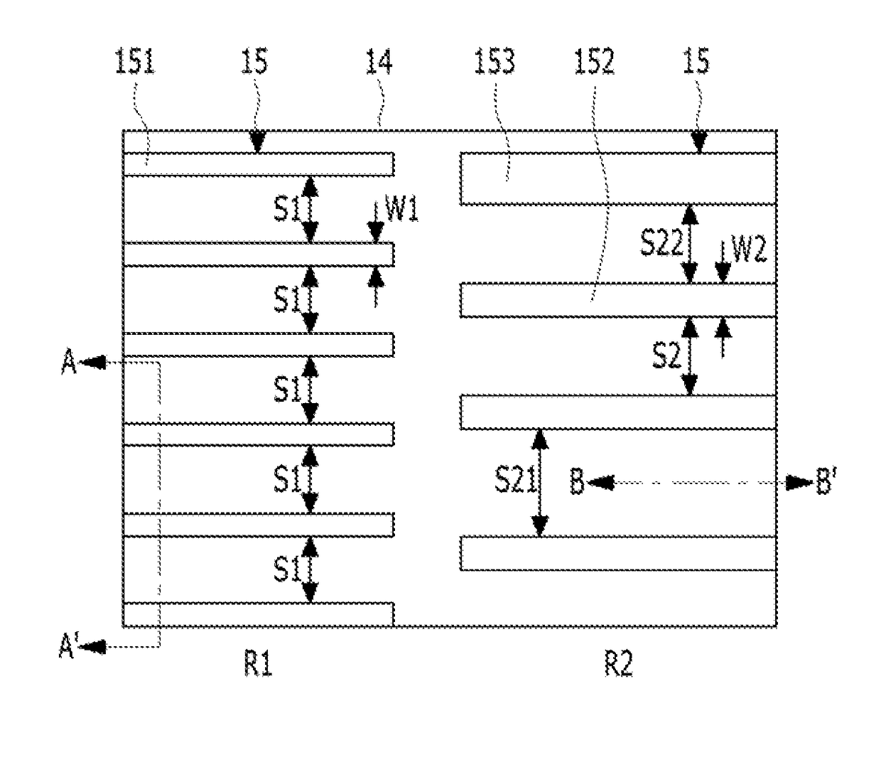
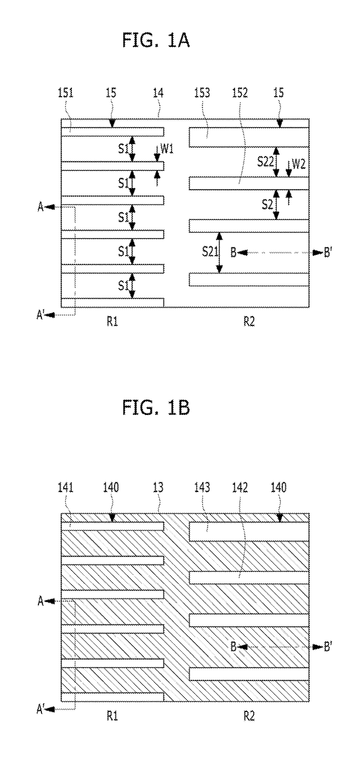
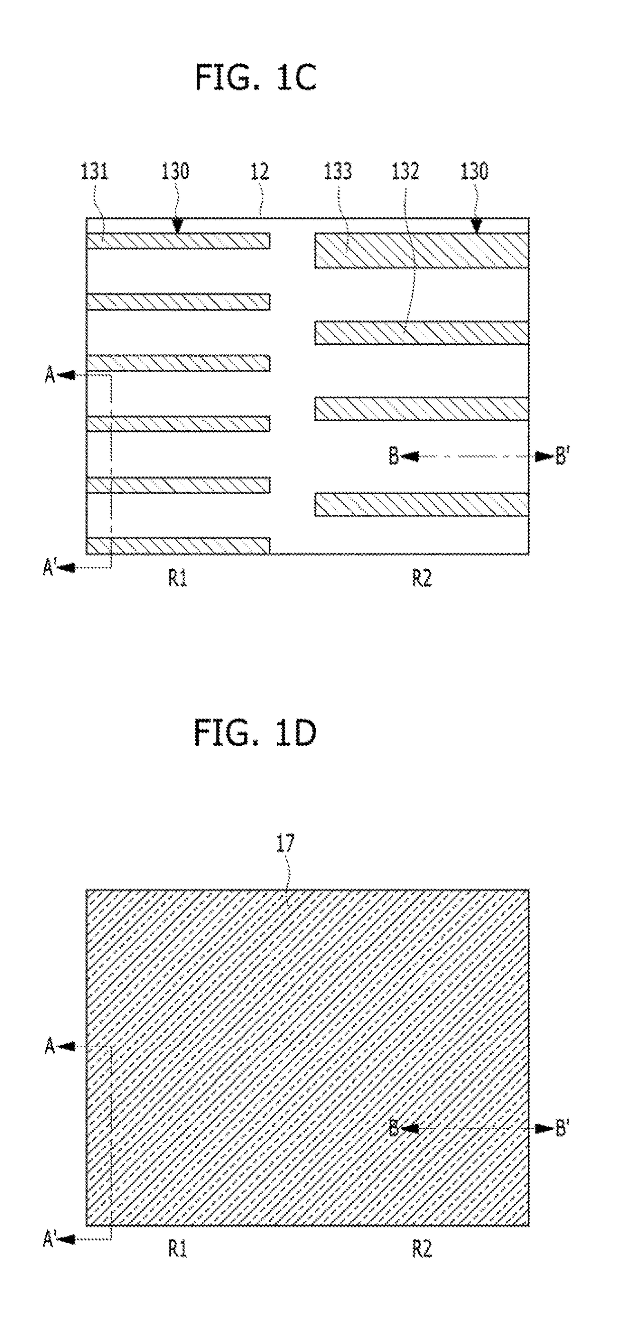
[0022]FIGS. 1A to 1O are plan views illustrating a method for forming patterns of a semiconductor device in accordance with a FIGS. 2A to 2O are cross-sectional views taken along the lines A-A′ and B-B′ of FIGS. 1A to 1O.

[0023]As shown in FIGS. 1A and 2A, an etch target layer 11 may be prepared. The etch target layer 11 may include suitable materials for semiconductor processing. The etch target layer 11 may include a semiconductor substrate. For example, the etch target layer 11 may include a silicon substrate, a silicon germanium (SiGe) substrate or an Silicon On Insulator (SOI) substrate. Also, the etch target layer 11 may include a dielectric material or a conductive material. For example, the etch target layer 11 may include a silicon oxide, a silicon nitride, a polysilicon, a metallic material, or a combination thereof. The etch target layer 11 may include a dielectric material which is formed on a semiconductor substrate.

[0024]The etch target layer 11 may include a first reg...

second embodiment

[0081]FIGS. 4A to 4P are plan views illustrating a method for forming patterns of a semiconductor device in accordance with a FIGS. 5A to 5P are cross-sectional views taken along the lines A-A′, B-B′ and C-C′ of FIGS. 4A to 4P.

[0082]As shown in FIGS. 4A and 5A, an etch target layer 31 may be prepared. The etch target layer 31 may include suitable materials for semiconductor processing. The etch target layer 31 may include a semiconductor substrate. For example, the semiconductor substrate may include a silicon substrate, a silicon germanium (SiGe) substrate or an Silicon On Insulator (SOI) substrate. Also, the etch target layer 31 may include a dielectric material or a conductive material. For example, the etch target layer 31 may include a silicon oxide, a silicon nitride, a polysilicon, a metallic material, or a combination thereof.

[0083]The etch target layer 31 may include a first region R1, a second region R2 and a third region R3. The first region R1 may be a region formed wit...


PUM


Abstract

A method for forming patterns of a semiconductor device includes preparing an etch target layer defined with a first region and a second region; forming a regular first feature which is positioned over the etch target layer in the first region and a random feature which is positioned over the etch target layer in the second region; forming a regular second feature over the regular first feature; forming first and second cutting barriers which expose a portion of the random feature, over the random feature; cutting the regular first feature using the regular second feature, to form a regular array feature; cutting the random feature using the first cutting barrier and the second cutting barrier, to form a random array feature; and etching the etch target layer by using the regular array feature and the random array feature, to form a regular array pattern and a random array pattern.

Description

CROSS-REFERENCE TO RELATED APPLICATION[0001]This application claims priority under 35 U.S.C. §119 to Korean Patent Application No. 10-2015-0105235 filed on Jul. 24, 2015, the disclosure of which is herein incorporated by reference in its entirety.TECHNICAL FIELD[0002]Exemplary embodiments relate to a method for manufacturing a semiconductor device, and more particularly, to a method for forming patterns.DISCUSSION OF THE RELATED ART[0003]Recently, the design rule of a semiconductor device is decreasing overall size. Thus, difficulties exist in forming patterns with fine pitches due to a limit in the resolution of a photolithography process.[0004]In order to overcome the limit in the resolution of a photolithography process, various patterning methods such as a spacer patterning technology (SPT) have been suggested.[0005]In this regard, it is necessary to develop a new process for concurrently forming fine patterns with different pattern densities in a region with a relatively high p...

Claims


Application Information

Patent Timeline
Patent Type & Authority Patents(United States)
IPC IPC(8): H01L21/033
CPCH01L21/0337H01L27/0207
Inventor KANG, CHUN-SOO
Owner SK HYNIX INC
Why Eureka
Try Eureka