Organic light emitting display device

a light-emitting display and organic technology, applied in the direction of organic semiconductor devices, solid-state devices, semiconductor devices, etc., can solve the problems of difficult to realize a uniform screen of organic light-emitting display devices, and achieve the effects of reducing color defects or color differences, and reducing color defects

Active Publication Date: 2018-01-02
LG DISPLAY CO LTD
View PDF6 Cites 0 Cited by
  • Summary
  • Abstract
  • Description
  • Claims
  • Application Information

AI Technical Summary

Benefits of technology

[0014]Through the various experiments, the inventors have invented a new organic light emitting display device for reducing a color defect or a color difference which occurs depending on positions at which an organic light emitting display device is seen.
[0015]An aspect of the present invention is directed to provide an organic light emitting display device in which a moving range of a peak wavelength of an electroluminescence (EL) spectrum of the organic light emitting display device is optimized, thereby reducing a color defect or a color difference which occurs in the front or side of the organic light emitting display device.
[0016]Another aspect of the present invention is directed to provide an organic light emitting display device that has a peak wavelength of EL spectrum (PWES) structure where a moving range of a peak wavelength of an EL spectrum of the organic light emitting display device is set, thereby reducing a color defect or a color difference which occurs in the front or side of the organic light emitting display device.

Problems solved by technology

However, since a peak wavelength of a spectrum is changed depending on a position at which an organic light emitting display device is seen, a color displayed on a screen of the organic light emitting display device is changed, and for this reason, it is difficult to realize a uniform screen of the organic light emitting display device.

Method used


Image

  • Organic light emitting display device
  • Organic light emitting display device
  • Organic light emitting display device

Examples


first embodiment

[0074]FIG. 1 is a schematic cross-sectional view illustrating an organic light emitting device 100 according to the present invention. The organic light emitting device 100 illustrated in FIG. 1 may have a patterned emission layer structure and may emit light having a mono color or the same wavelength range. The patterned emission layer structure may have a structure where a plurality of emission layers (for example, a red (R) emission layer, a green (G) emission layer, and a blue (B) emission layer) which respectively emit lights having different colors are divisionally provided in a plurality of pixels, respectively, and each of the plurality of pixels may emit light having a mono color or the same wavelength range. Each of the plurality of emission layers may be pattern-deposited in a corresponding pixel by using an opened mask (for example, a fine metal mask (FMM)). For convenience of description, only a structure where the organic light emitting device 100 is disposed in one pi...

second embodiment

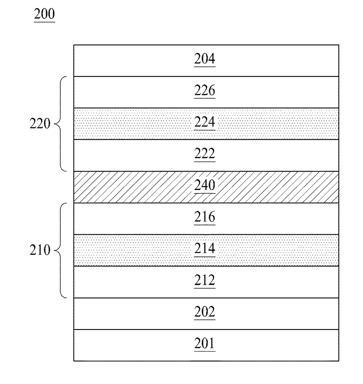
[0090]FIG. 2 is a schematic cross-sectional view illustrating an organic light emitting device 200 according to the present invention. The organic light emitting device 200 illustrated in FIG. 2 may have a patterned emission layer structure and may emit light having a mono color or the same wavelength range. The patterned emission layer structure may have a structure where a plurality of emission layers (for example, a red (R) emission layer, a green (G) emission layer, and a blue (B) emission layer) which respectively emit lights having different colors are divisionally provided in a plurality of pixels, respectively, and each of the plurality of pixels may emit light having a mono color or the same wavelength range. Each of the plurality of emission layers may be pattern-deposited in a corresponding pixel by using an opened mask (for example, an FMM). For convenience of description, only a structure where the organic light emitting device 200 is disposed in one pixel is illustrate...

third embodiment

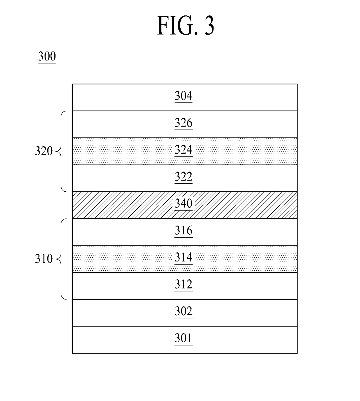
[0108]FIG. 3 is a schematic cross-sectional view illustrating an organic light emitting device 300 according to the present invention.

[0109]The organic light emitting device 300 illustrated in FIG. 3 may include a first electrode 302, a second electrode 304, a first emission part 310, and a second emission part 320 which are disposed on a substrate 301. The first and second emission parts 310 and 320 may be disposed between the first electrode 302 and the second electrode 304. The substrate 301, the first electrode 302, and the second electrode 304 illustrated in FIG. 3 may be substantially the same as the substrate 101, the first electrode 102, and the second electrode 104 described above with reference to FIG. 1. Thus, detailed descriptions of the substrate 301, first electrode 302, and second electrode 304 of FIG. 3 are omitted.

[0110]The first emission part 310 may include a first HTL 312, a first EML 314, and a first ETL 316 which are disposed on the first electrode 302.

[0111]An...


PUM


Abstract

Discussed is an organic light emitting display device for reducing a color defect or a color difference which occurs in the front or side of the organic light emitting display device. The organic light emitting display device can include a first electrode, a second electrode and an organic layer between the first electrode and the second electrode, the organic layer including at least one emission part. The organic layer is configured for a peak wavelength of an electroluminescence (EL) spectrum of the organic light emitting display device emitted from the at least one emission part to have a range from 10 nm less a predetermined peak wavelength to 10 nm more than the predetermined peak wavelength.

Description

CROSS-REFERENCE TO RELATED APPLICATIONS[0001]This application claims the priority benefit of the Korean Patent Application No. 10-2014-0158315 filed on Nov. 13, 2014 and the Korean Patent Application No. 10-2015-0138248 filed on Sep. 30, 2015. All of these applications are hereby incorporated by reference as if fully set forth herein.BACKGROUND OF THE INVENTION[0002]Field of the Invention[0003]The present invention relates to an organic light emitting display device, and more particularly, to an organic light emitting display device for reducing a color defect or a color difference which occurs in the front or side of the organic light emitting display device.[0004]Discussion of the Related Art[0005]Recently, as society advances to the information-oriented society, the field of display devices which visually express an electrical information signal is rapidly advancing. Various types of display devices, having excellent performance in terms of thinning, lightening, and low power con...

Claims


Application Information

Patent Timeline
Patent Type & Authority Patents(United States)
IPC IPC(8): H01L51/52H01L51/50H01L27/32
CPCH01L51/5278H01L51/504H01L2251/558H01L51/5265H01L27/3209H10K59/30H10K59/32H10K50/852H10K50/19H10K2102/351H10K50/12H10K50/125H10K50/11H10K59/10H10K50/13
Inventor SONG, KI-WOOGHEO, JEONGHAENGKUM, TAEILKIM, SEUNGCHOI, HEEDONGKIM, HYUNGJUNE
Owner LG DISPLAY CO LTD
Why Eureka
Try Eureka