
Display device

a display device and chip-on-plastic technology, applied in non-linear optics, instruments, optics, etc., can solve problems such as defects in driving elements and compression defects, and achieve the effect of suppressing crack formation in an insulating layer and reducing compression defects

Active Publication Date: 2018-01-09
SAMSUNG DISPLAY CO LTD
View PDF15 Cites 0 Cited by
  • Summary
  • Abstract
  • Description
  • Claims
  • Application Information

AI Technical Summary

Benefits of technology

The present invention is about a display device that can prevent defects and crack formation during a compression process of a panel and a driving chip. This invention helps to reduce deformation of the display panel and minimize the occurrence of compression defects and insulating layer cracking, which can prolong the life of the display device and improve its overall performance.

Problems solved by technology

However, in the COG method, organic insulating layers and the like are stacked as a protection layer so as to protect a driving element such as a TFT of an organic light emitting diode (OLED) display device, and thus compression defects may occur when connecting a bump and the like to a pad unit due to a step difference between the pad unit, below which a metal layer is disposed, and portions apart from the pad unit.
In a case where the flexible OLED display device retains its curved shape, however, a crack may appear on the insulating layer protecting the TFT, thus causing a defect in the driving element.

Method used


Image

  • Display device
  • Display device
  • Display device

Examples


Embodiment Construction

[0041]Aspects and features of the present invention and methods for achieving them will be made clear from embodiments described below in detail with reference to the accompanying drawings. The present invention may, however, be embodied in many different forms and should not be construed as being limited to the embodiments set forth herein. Rather, these embodiments are provided so that this disclosure will be thorough and complete, and will fully convey the scope of the invention to those skilled in the art. The present invention is merely defined by the scope of the claims and equivalents thereof. Therefore, well-known constituent elements, operations and techniques are not described in detail in the embodiments in order to prevent the present invention from being obscurely interpreted. Like reference numerals refer to like elements throughout the specification.

[0042]The spatially relative terms “below”, “beneath”, “lower”, “above”, “upper”, and the like, may be used herein for e...


PUM

PropertyMeasurementUnit
angleaaaaaaaaaa
diameteraaaaaaaaaa
areaaaaaaaaaaa

Abstract

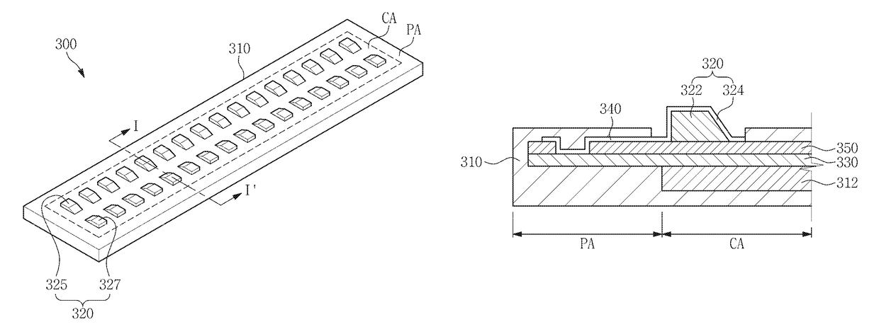
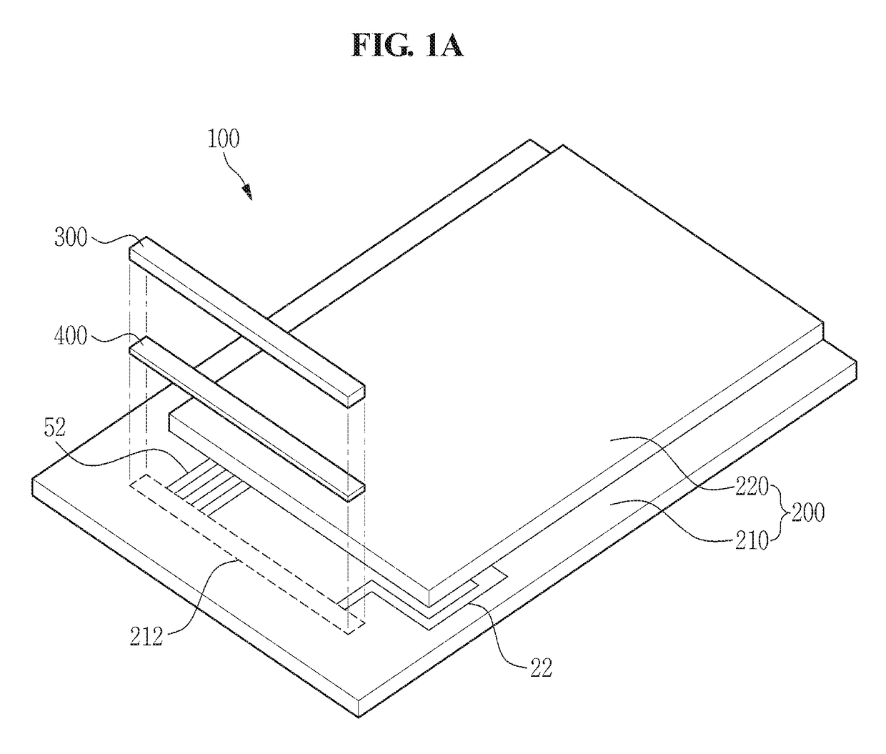
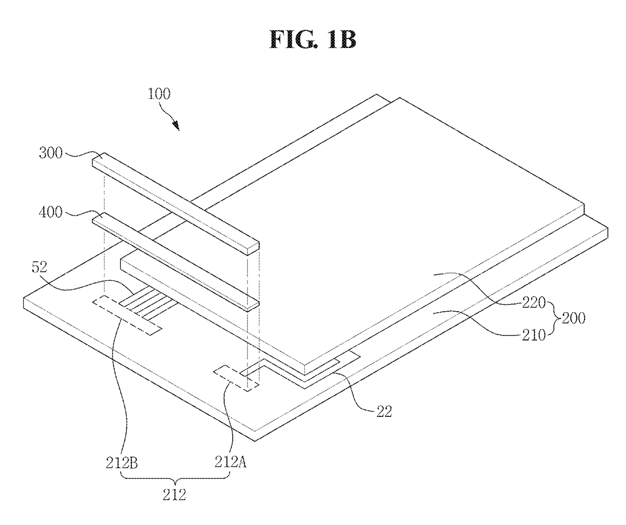
A display device includes: a display panel including a display area and a non-display area; a at least one pad in the non-display area of the display panel; a driving chip connected to the at least one pad, the driving chip including a driving circuit and at least one bump therein, wherein the at least one bump has an inclined surface facing toward a central portion of the driving chip.

Description

CROSS-REFERENCE TO RELATED APPLICATION[0001]This application claims priority to and the benefit of Korean Patent Application No. 10-2015-0052447, filed on Apr. 14, 2015, with the Korean Intellectual Property Office (KIPO), the disclosure of which is incorporated herein in its entirety by reference.BACKGROUND[0002]1. Field[0003]Aspects of embodiments of the present invention relate to a display device, and more particularly, to a chip on plastic (COP) type display device.[0004]2. Description of the Related Art[0005]Embodiments of the present invention are directed to a liquid crystal display (LCD) device, in more particular, to a COP type LCD device.[0006]The LCD device may display image information utilizing an electro-optical property of liquid crystal molecules injected into a liquid crystal panel provided therein. The LCD device may be advantageous over electronic products including a cathode ray tube (CRT) in that it has low power consumption, light weight, and a small volume. A...

Claims


Application Information

Patent Timeline
Patent Type & Authority Patents(United States)
IPC IPC(8): G02F1/1345
CPCG02F1/13452G02F1/13454G02F2001/13456G02F1/13456
Inventor LEE, DAEGEUN
Owner SAMSUNG DISPLAY CO LTD
Learn More