Method for forming shallow trenches of the dual active regions

a dual active and trenching technology, applied in the field of new, trenching method of dual active regions, can solve the problems of increasing cost and great difficulty in refilling ability, and achieve the effect of low cos

Active Publication Date: 2018-01-16
SHANGHAI HUALI MICROELECTRONICS CORP
View PDF3 Cites 0 Cited by
  • Summary
  • Abstract
  • Description
  • Claims
  • Application Information

AI Technical Summary

Benefits of technology

[0033]Concluded from the above technical solutions, in order to meet the needs of two different etching depths of shallow trench in different regions for certain special chip design, firstly, the present invention uses a first accurate photomask to etch the etch stop layer, secondly, adopting the low-cost second photomask to accomplish the subsequent etching processes, wherein the in-situ stripping process is utilized to complete the integral etching of shallow trench regions with two different depths. The present invention has realized a low-cost photomask application and an optimization of the etching process by optimizing the photomask design, and has provided a new solution for the shallow trench process of the dual active regions.

Problems solved by technology

However, above solutions of the prior art exist some problems, which are:
1) the two accurate photomasks are needed which increases the cost;
2) the shallow trench depths at the active regions of the CMOS image sensors after the first etching process will bring great difficulties for the refilling ability and flatness of the BARC layer 1 (bottom anti-reflective coating) of the second accurate photomask.

Method used


Image

  • Method for forming shallow trenches of the dual active regions
  • Method for forming shallow trenches of the dual active regions
  • Method for forming shallow trenches of the dual active regions

Examples


Embodiment Construction

[0041]The present invention will be described in further details hereinafter by referring to the accompanying drawings, so as to provide a better understanding of the present invention.

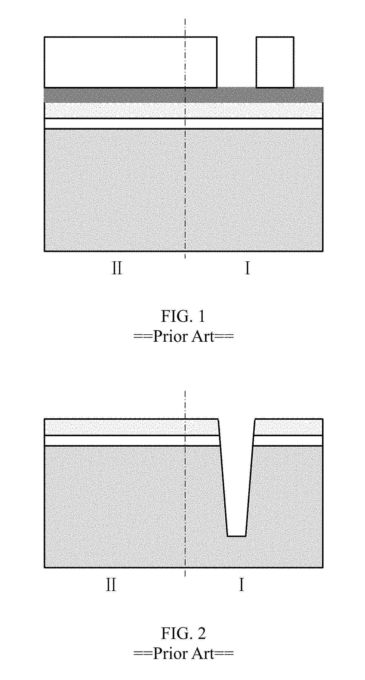
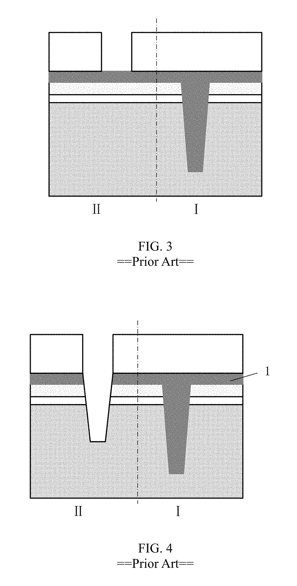
[0042]It should be noted that, in the following specific embodiments, when these embodiments of the present invention are described in detail, in order to clearly illustrate the structure of the present invention to facilitate explanation, the accompanying drawings are not necessarily drawn to scale, some features in the drawings may have been fragmentary enlarged, deformed or simplified. Therefore, it would be avoided to understand this as a limitation to the present invention.

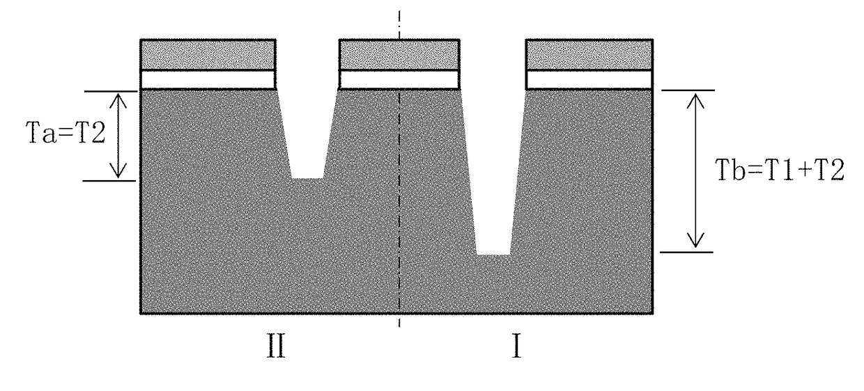
[0043]Referring to FIG. 6, which is a flow sheet illustrating the shallow trench forming method of the dual active regions of the present invention. As shown in FIG. 6, which discloses a method for forming shallow trenches of the dual active regions, comprising the steps of

[0044]Executing Step S01: providing a semiconductor sub...


PUM


Abstract

The invention disclosed a method for forming shallow trenches of the dual active regions. Firstly, forming an etch stop layer on a semiconductor substrate; secondly, using a first accurate photomask to expose and develop the semiconductor substrate, until the etch stop layer has been exposed on the top of the first shallow trench regions and the second shallow trench regions; thirdly, etching the etch stop layer entirely in the exposed regions; fourthly, using a second photomask to expose and develop the first shallow trench regions which require a deeper etch depth of the trench than that of the second shallow trench regions; fifthly, etching and forming preliminary entirely depth in the first shallow trench regions, and then removing the second photomask; at last, taking the etch stop layer as a mask, and simultaneously etching the first shallow trench regions and the second shallow trench regions to form the first hallow trenches and the second shallow trenches having different depths. The invention has realized a low-cost photomask application and an optimization of the etching process by optimizing the photomask design.

Description

CROSS-REFERENCE TO RELATED APPLICATION[0001]This application claims the priority benefit of China patent application serial No. 201610604747.7, filed Jul. 28, 2016. The entire contents of the above-mentioned patent application are hereby incorporated by reference herein and made a part of the specifications.FIELD OF THE INVENTION[0002]The present invention relates to the field of semiconductor manufacturing technology, and particularly to a new method for forming shallow trenches of the dual active regions.BACKGROUND OF THE INVENTION[0003]CMOS image sensors are electrical solid-state imaging sensors, which are exhibiting more superiority in the aspects of system complexity and reliability, data output and exposure control, etc., than traditional CCD, due to their intrinsic high integration. Therefore, audio and video products based the CMOS image sensors will replace the CCD products to become the main trend of market in the future.[0004]In the semiconductor manufacturing process, t...

Claims


Application Information

Patent Timeline
Patent Type & Authority Patents(United States)
IPC IPC(8): H01L21/00H01L27/146H01L21/31H01L21/311H01L21/762H01L21/3213H01L21/04H01L21/027
CPCH01L27/1461H01L27/14687H01L21/3213H01L21/0475H01L21/0274H01L21/31116H01L21/76229H01L21/31H01L21/027H01L21/76H01L21/02057H01L21/31138
Inventor JING, QUANXU, JINCHEN, MINJIEREN, YULV, YUKUNZHU, JUNZHANG, XUSHENG
Owner SHANGHAI HUALI MICROELECTRONICS CORP
Why Eureka
Try Eureka