
Techniques for fabricating horizontally aligned nanochannels for microfluidics and biosensors

a nanochannel and nanopore technology, applied in the field of nanochannel devices, can solve the problems of incompatibility with large-scale integration, device unsatisfactory from an application point of view, and difficult fabrication of nanochannels or nanopores with ultra-thin alternating layer properties (i.e., multi-layers of insulators/metals) in the nanoscale rang

Active Publication Date: 2018-02-13
INT BUSINESS MASCH CORP
View PDF15 Cites 0 Cited by
  • Summary
  • Abstract
  • Description
  • Claims
  • Application Information

AI Technical Summary

Benefits of technology

This patent describes a method for making a device with tiny channels that are aligned horizontally. The method involves forming a layer of silicon on insulator, attaching nanowires to pads, and then suspending them over the insulator. A mask is made with a gap where the nanowire is exposed. An alternating series of metal layers and insulator layers is formed within the gap and around the nanowire, and the nanowire is removed to create the channels. The resulting device has a layered structure with metal and insulator layers that provide support for the channels. This invention provides a way to make complex devices with precise channel alignments, which could be useful in various fields such as electronics or sensors.

Problems solved by technology

Nanochannels or nanopores with ultra-thin alternating layer properties (i.e., multi-layers of insulator / metal) are very challenging to be fabricated in the nanoscale range (e.g., less than 10 nanometer (nm) channel diameter).
While solutions exist to fabricate vertically aligned nanochannels / nanopores, for instance, using highly focused electron beam (e-beam), such as the e-beams used in ultra-high resolution transmission electron microscopy (TEM) systems, to drill individual nanopores on a very small sample, typical sample sizes being less than 10 millimeters (mm)×10 mm, these devices are not ideal from an application point of view.
Furthermore, the solutions are not compatible with large scale integration, thus preventing the advantage of lowering production costs.
The hole drilling process is not compatible with large scale integration, and also the vertical alignment is unfavorable.
This makes the fabrication of these biosensors very expensive and is in contrast to the original idea that processing sensors using silicon process technology would bring down the cost per sensor.

Method used


Image

  • Techniques for fabricating horizontally aligned nanochannels for microfluidics and biosensors
  • Techniques for fabricating horizontally aligned nanochannels for microfluidics and biosensors
  • Techniques for fabricating horizontally aligned nanochannels for microfluidics and biosensors

Examples


Embodiment Construction

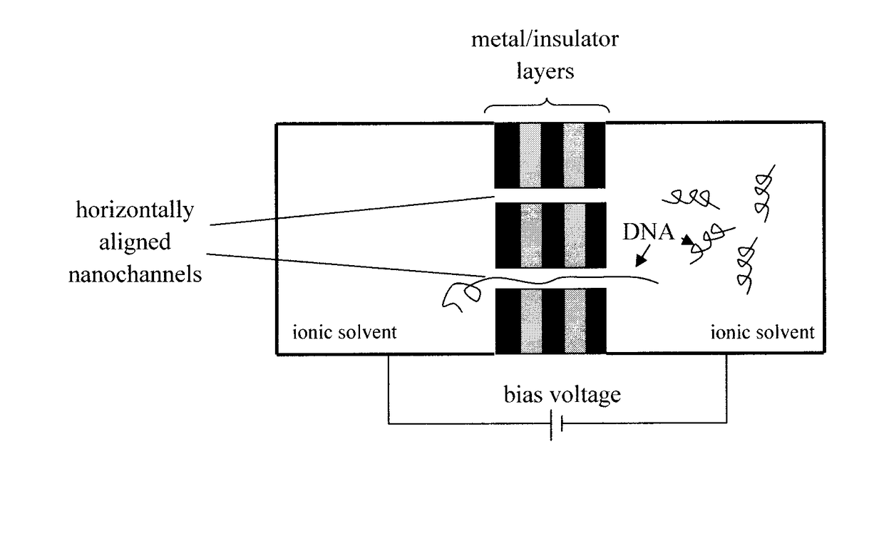
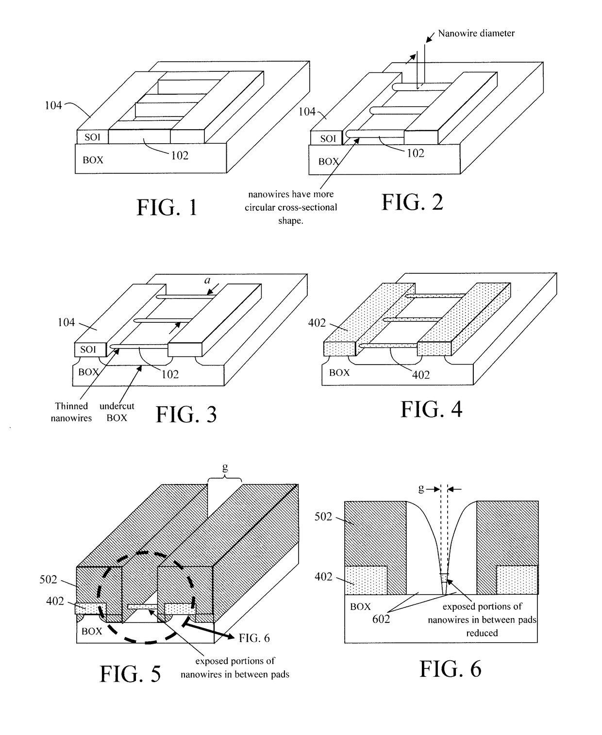
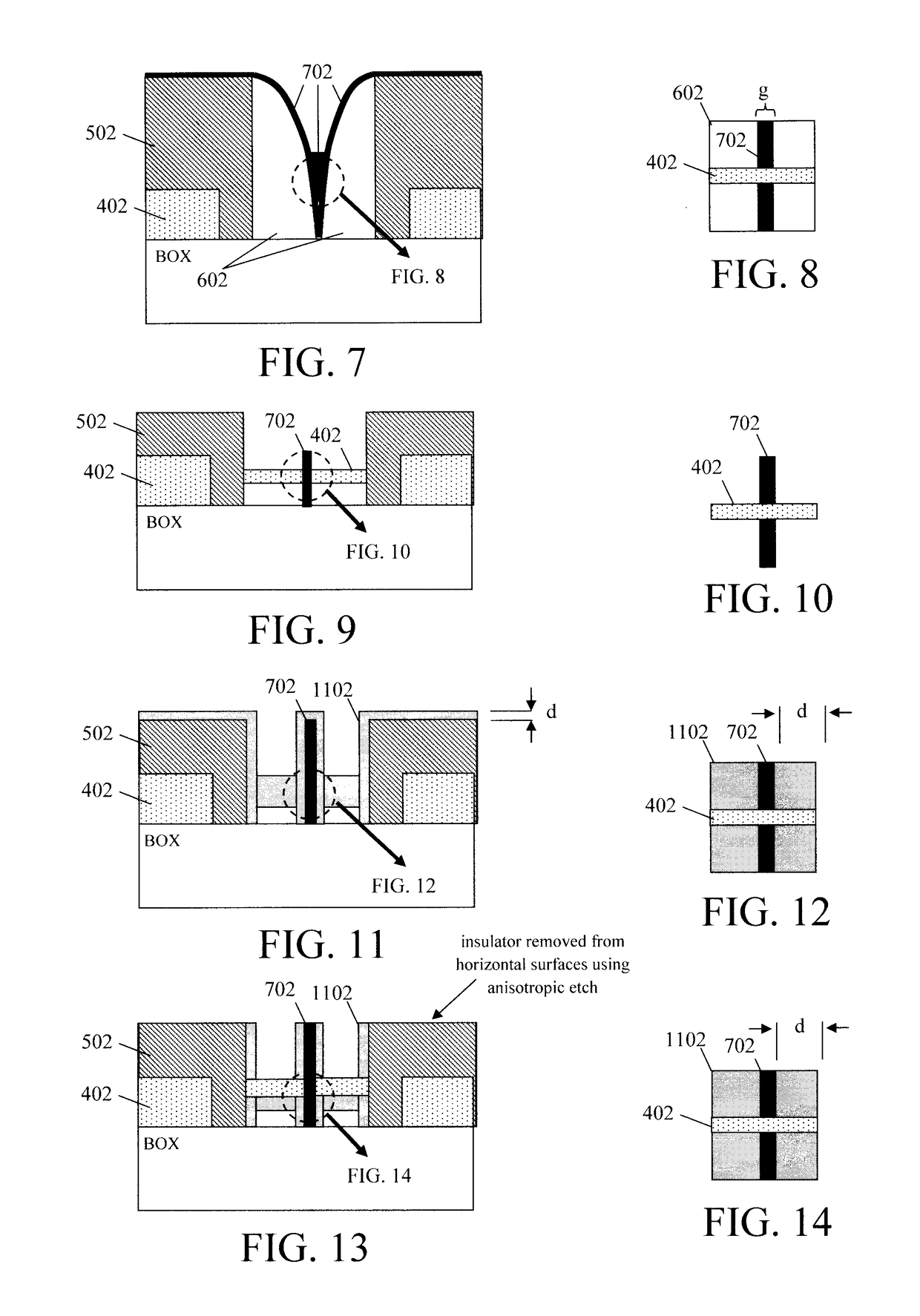
[0045]Provided herein are techniques for fabricating horizontally aligned nanochannels useful for a variety of applications. As will be described in detail below, the present techniques leverage the accessibility of a nanowire to recess a whole layer of thickness d from the nanowire, where etching on the extent of d / 2 occurs from 2 fronts. The same amount of etch has to be expected on the sidewall, leaving d / 2 of the original deposited thickness d on the sidewall. By repeating the above procedure, alternating layers of very fine thickness can be deposited around a dummy wire. The dummy wire can then be selectively removed to form the nanofluidic nanochannels.

[0046]A first exemplary embodiment of the present techniques are now described in detail by way of reference to FIGS. 1-26. As shown in FIG. 1, the process begins with a wafer in which at least one nanowire 102 has been defined. According to the exemplary embodiment shown illustrated in the figures, the starting wafer is a silic...


PUM

PropertyMeasurementUnit
sizesaaaaaaaaaa
sizesaaaaaaaaaa
temperatureaaaaaaaaaa

Abstract

Techniques for fabricating horizontally aligned nanochannels are provided. In one aspect, a method of forming a device having nanochannels is provided. The method includes: providing a SOI wafer having a SOI layer on a buried insulator; forming at least one nanowire and pads in the SOI layer, wherein the nanowire is attached at opposite ends thereof to the pads, and wherein the nanowire is suspended over the buried insulator; forming a mask over the pads, the mask having a gap therein where the nanowire is exposed between the pads; forming an alternating series of metal layers and insulator layers alongside one another within the gap and surrounding the nanowire; and removing the nanowire to form at least one of the nanochannels in the alternating series of the metal layers and insulator layers. A device having nanochannels is also provided.

Description

CROSS-REFERENCE TO RELATED APPLICATION(S)[0001]This application is a continuation of U.S. application Ser. No. 15 / 192,281 filed on Jun. 24, 2016, the contents of which are incorporated by reference herein as if fully set forth herein.FIELD OF THE INVENTION[0002]The present invention relates to devices having nanochannels, and more particularly, to techniques for fabricating horizontally aligned nanochannels.BACKGROUND OF THE INVENTION[0003]Nanochannels or nanopores with ultra-thin alternating layer properties (i.e., multi-layers of insulator / metal) are very challenging to be fabricated in the nanoscale range (e.g., less than 10 nanometer (nm) channel diameter). While solutions exist to fabricate vertically aligned nanochannels / nanopores, for instance, using highly focused electron beam (e-beam), such as the e-beams used in ultra-high resolution transmission electron microscopy (TEM) systems, to drill individual nanopores on a very small sample, typical sample sizes being less than 1...

Claims


Application Information

Patent Timeline
Patent Type & Authority Patents(United States)
IPC IPC(8): G01N27/403B82B3/00B82B1/00G01N27/414G01N33/487
CPCG01N27/4146B82B1/005G01N33/48721G01N27/4145B82B3/008B01L3/502761B81C1/00119B01L2200/0663B81B2201/051B81C2201/0181B01L3/502707B01L2300/0896B01L2300/0861B01L2300/0887
Inventor ENGELMANN, SEBASTIAN U.ROSSNAGEL, STEPHEN M.ZHANG, YING
Owner INT BUSINESS MASCH CORP
Learn More