Supercharge Your Innovation With Domain-Expert AI Agents!

Resistive memory device and a memory system including the same

a technology of resistive memory and memory system, which is applied in the direction of information storage, static storage, digital storage, etc., can solve the problems of performance degradation and lowered read performan

Active Publication Date: 2018-02-20
SAMSUNG ELECTRONICS CO LTD
View PDF9 Cites 3 Cited by
  • Summary
  • Abstract
  • Description
  • Claims
  • Application Information

AI Technical Summary

Problems solved by technology

For example, when data of a unit cell of a resistive memory is read, a relatively large amount of time may be required to secure a predetermined sensing margin, and thus, read performance may be lowered.
Performance degradation may occur due to various causes, such as a variation in a manufacturing process of a semiconductor memory device or a variation in a signal that is provided to various circuits (for example, data write or read circuits) for operating the semiconductor memory device.

Method used


Image

  • Resistive memory device and a memory system including the same
  • Resistive memory device and a memory system including the same
  • Resistive memory device and a memory system including the same

Examples


Embodiment Construction

[0033]Exemplary embodiments of the inventive concept will be described more fully hereinafter with reference to the accompanying drawings. Like reference numerals may refer to like elements throughout the accompanying drawings.

[0034]Exemplary embodiments of the inventive concept provide a memory device and a memory system including the memory device capable of increasing performance of read operations.

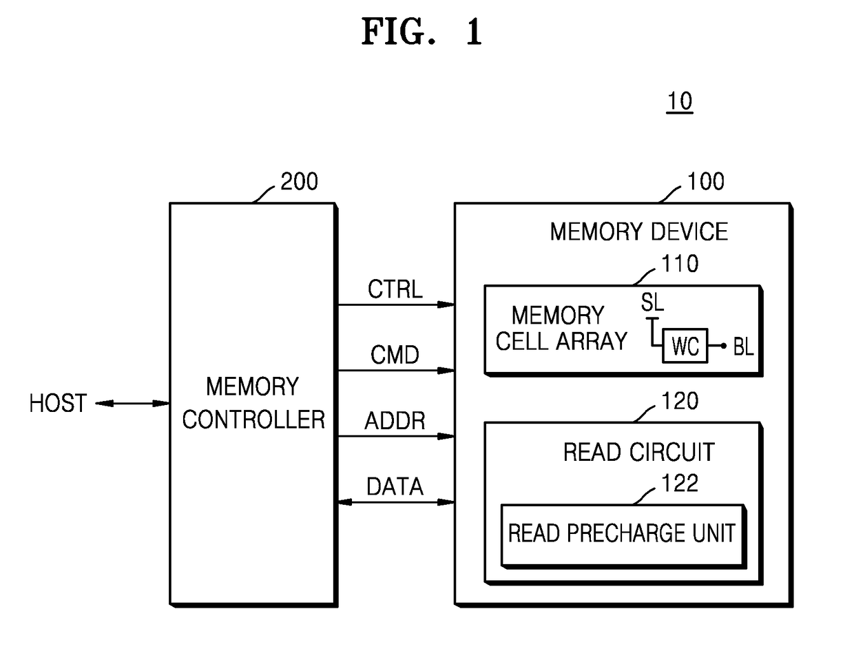
[0035]FIG. 1 is a block diagram of a memory system 10 according to an exemplary embodiment of the inventive concept.

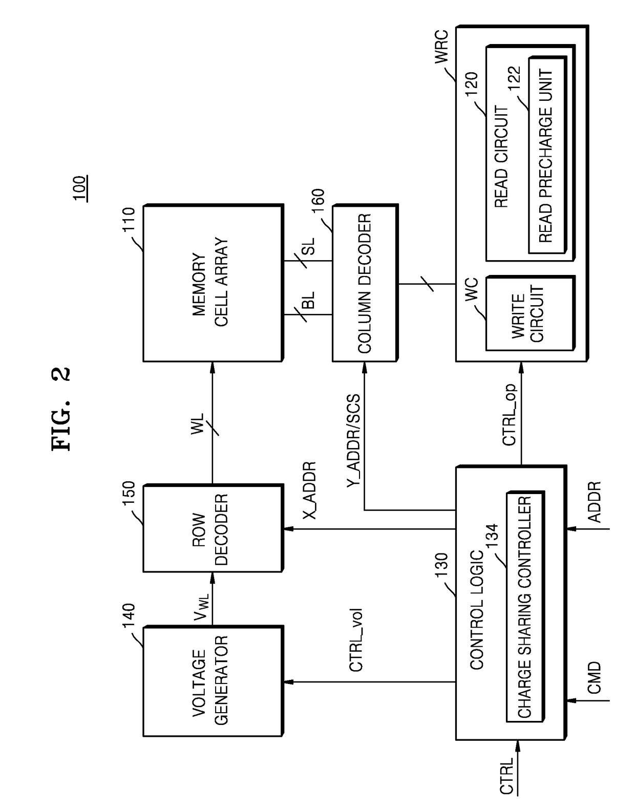
[0036]Referring to FIG. 1, the memory system 10 may include a memory device 100 and a memory controller 200. The memory device 100 may include a memory cell array 110 and a read circuit 120.

[0037]In response to a write / read request from a host HOST, the memory controller 200 may read data stored in the memory device 100 or may write data to the memory device 100. For example, the memory controller 200 may provide an address ADDR, a command CMD, and a control signal CTRL t...


PUM


Abstract

A memory device includes a memory cell array, a read circuit, and a control logic. The memory cell array includes a memory cell having a resistance level that varies depending on data stored therein. The memory cell is connected to a first signal line and a second signal line. The read circuit is configured to read the data. The control logic is configured to precharge a sensing node, connected to the first signal line through a first switching device, and a first node, connected to the second signal line through a second switching device, to different voltage levels during a first period, and develop a voltage of the sensing node based on the resistance level of the memory cell during a second period.

Description

CROSS-REFERENCE TO RELATED APPLICATION[0001]This application claims priority under 35 U.S.C. § 119 to Korean Patent Application No. 10-2016-0048962, filed on Apr. 21, 2016 in the Korean Intellectual Property Office, the disclosure of which is incorporated by reference herein in its entirety.TECHNICAL FIELD[0002]Exemplary embodiments of the inventive concept relate to a resistive memory device, and more particularly, to a resistive memory device for reading data of resistive memory cells and a memory system including the resistive memory device.DISCUSSION OF RELATED ART[0003]Semiconductor memory devices, which are devices for storing information, may be classified into two categories: volatile memory devices and non-volatile memory devices. Examples of non-volatile memory devices may include phase change random access memory (PRAM), resistive random access memory (RRAM), magnetic random access memory (MRAM), and ferroelectric random access memory (FRAM). The RRAM may use a material w...

Claims


Application Information

Patent Timeline
Patent Type & Authority Patents(United States)
IPC IPC(8): G11C11/00G11C13/00
CPCG11C13/004G11C13/0026G11C13/0097G11C13/0064G11C13/0069G11C13/0028G11C11/1655G11C11/1673G11C13/0004G11C13/0007G11C13/0061G11C11/1675G11C2013/0045G11C2213/79G11C2213/82G11C11/1677G11C11/1693G11C13/0021G11C13/0002G11C2213/74
Inventor PYO, SUK-SOO
Owner SAMSUNG ELECTRONICS CO LTD
Features
  • R&D
  • Intellectual Property
  • Life Sciences
  • Materials
  • Tech Scout
  • Unparalleled Data Quality
  • Higher Quality Content
  • 60% Fewer Hallucinations
Learn More