Substrate structure and manufacturing method thereof

a technology of substrate structure and manufacturing method, which is applied in the direction of semiconductor devices, semiconductor/solid-state device details, electrical apparatus, etc., can solve the problems of difficult narrowing the aperture of blind holes and inability to achieve circuits with fine pitch, and achieve low-cost and high-electric effects

Active Publication Date: 2018-04-10
PHOENIX PIONEER TECH
View PDF1 Cites 0 Cited by
  • Summary
  • Abstract
  • Description
  • Claims
  • Application Information

AI Technical Summary

Benefits of technology

[0009]In view of the foregoing, the present invention is to provide a substrate structure and its manufacturing method having rigidity and heat dissipation and meeting the fine line spacing, high-density, thinning tendency, low-cost and high electric characteristics.

Problems solved by technology

Thus, electronics manufacturers have to accommodate more components in a limited space of an integrated circuit (IC) to achieve high density and miniaturization.
It is difficult to narrow the aperture of the blind hole by laser drilling or mechanical drilling and cannot achieve the circuit with the fine pitch.

Method used


Image

  • Substrate structure and manufacturing method thereof
  • Substrate structure and manufacturing method thereof
  • Substrate structure and manufacturing method thereof

Examples


Embodiment Construction

[0029]Reference will now be made to the drawings to describe various inventive embodiments of the present disclosure in detail, wherein like numerals refer to like elements throughout.

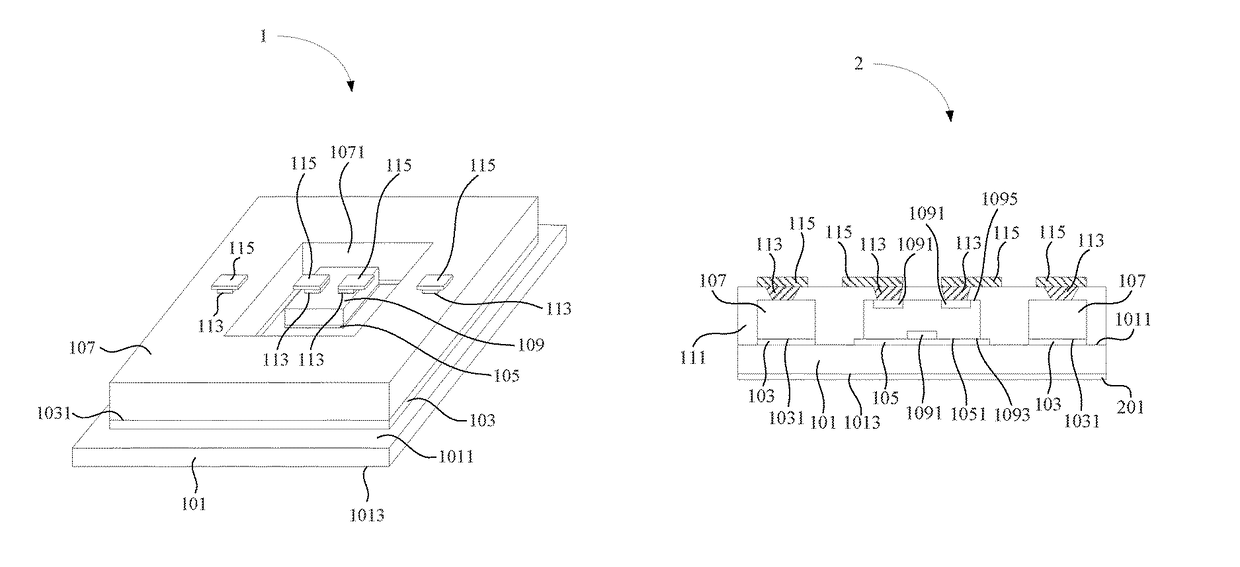
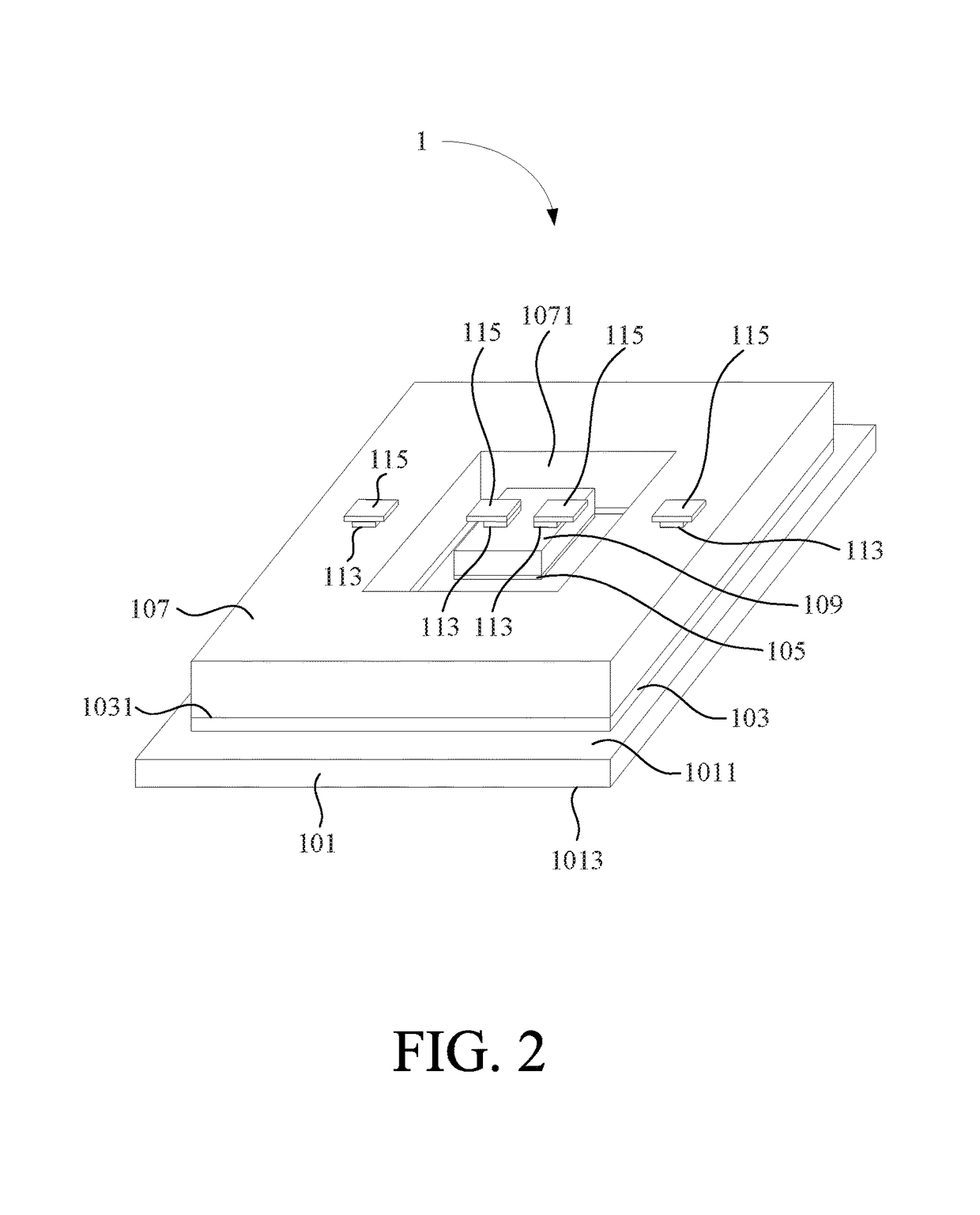
[0030]FIG. 1, FIG. 2 and FIG. 3 depict a first embodiment of the present invention. FIG. 1 is a schematic diagram of a substrate structure 1 and FIG. 2 is a schematic diagram of a part of substrate structure 1. FIG. 3 is a sectional diagram of A-A′ line of FIG. 1. The substrate structure 1 comprises a metal substrate 101, a first connection layer 103, a second connection layer 105, a metal core layer 107, an internal component 109, a dielectric material layer 111, a conductive pillar layer 113 and a conductive wiring layer 115. The metal substrate 101 has a first surface 1011 and a second surface 1013. The first connection layer 103 has a surface 1031. The second connection layer 105 has a surface 1051. The metal core layer 107 has an opening 1071. The internal component 109 has a plurality of electrod...


PUM

PropertyMeasurementUnit
dielectricaaaaaaaaaa
structureaaaaaaaaaa
conductiveaaaaaaaaaa

Abstract

A substrate structure includes a metal substrate, a first connection layer, a second connection layer, a dielectric material layer, a metal core layer and an internal component. The first and second connection layers are disposed on a surface of the metal substrate. The metal core layer having an opening is disposed on a surface of the first connection layer. The internal component having a plurality of electrode pads is disposed on a surface of the second connection layer and in the opening of the metal core layer. The dielectric material layer is disposed on the surface of the metal substrate. The first and second connection layers, the metal core layer and the internal component are partially covered with the dielectric material layer. The metal core layer is electrically connected to one of the electrode pads via the first and second connection layers and the metal core layer.

Description

CROSS REFERENCE TO RELATED APPLICATIONS[0001]This Non-provisional application claims priority under 35 U.S.C. § 119(a) on Patent Application No. 105130268 filed in Taiwan on Sep. 20, 2016, the entire contents of which are hereby incorporated by reference.BACKGROUND1. Technical Field[0002]This invention relates to a substrate structure and a manufacturing method thereof, in particular, to a semiconductor substrate structure and a manufacturing method thereof.2. Description of Related Art[0003]In recent years, users prefer electronic products with compact size, high performance and versatility. Thus, electronics manufacturers have to accommodate more components in a limited space of an integrated circuit (IC) to achieve high density and miniaturization. As a result, electronics manufacturers advance a new IC package for embedding components in a substrate to reduce the package size and the connection path between the components and the substrate.[0004]A chip scale package (CSP) is a t...

Claims


Application Information

Patent Timeline
Patent Type & Authority Patents(United States)
IPC IPC(8): H01L23/02H01L23/06H01L21/50H01L23/532H01L21/768H01L23/34H01L21/44H01L23/528
CPCH01L23/528H01L23/53228H01L21/76885H01L2224/48091H01L23/5389H01L2224/32245H01L2224/73267H01L2224/04105H01L24/19H01L24/20H01L24/32H01L24/73H01L24/83H01L24/92H01L2224/06181H01L2224/83192H01L2224/92244H01L2924/3025H01L2924/3511H01L2224/8203H01L23/142H01L2924/00014
Inventor HSU, SHIH-PING
Owner PHOENIX PIONEER TECH
Why Eureka
Try Eureka