Insulated die

a technology of insulating die and adhesive body, which is applied in the direction of electrical apparatus, semiconductor devices, semiconductor/solid-state device details, etc., can solve the problems of deteriorating the reliability of the package, difficult to precisely adjust the properties of such electrically insulating adhesive body, and many conventionally used adhesive materials with insufficient electrically insulating properties, etc., to achieve reliable protection against creep current, high disruptive strength, and robust and efficient

Active Publication Date: 2018-05-22
INFINEON TECH AG
View PDF13 Cites 23 Cited by
  • Summary
  • Abstract
  • Description
  • Claims
  • Application Information

AI Technical Summary

Benefits of technology

[0007]There may be a need for a chip and a package with a chip which provide a high disruptive strength and a reliable protection against creep currents. Additionally or alternatively, there may be also a need for a chip and a package with a chip which are manufacturable by a robust and efficient manufacturing process and provide a reliable protection of the chip during processing.

Problems solved by technology

However, it is difficult to precisely adjust properties of such electrically insulating adhesive body (in particular in terms of dimensions, process stability, etc.).
Additionally, many conventionally used adhesive materials have insufficient electrically insulating properties, in particular when a high disruptive strength is required.
Consequently, conventional packages may suffer from the problem that undesired creep currents can flow, under undesired circumstances such as delamination, between an encapsulated electronic chip and another electrically conductive structure (such as another electronic chip, a trace, a via, etc.) of the package, which may deteriorate reliability of the package.

Method used


Image

  • Insulated die
  • Insulated die
  • Insulated die

Examples


Embodiment Construction

[0016]In the following, further exemplary embodiments of the insulated chip, the packages and the methods will be explained.

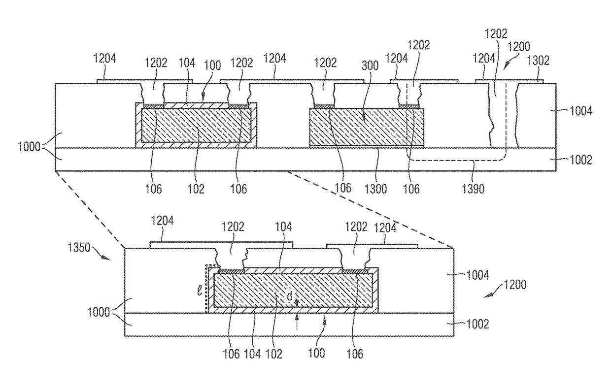
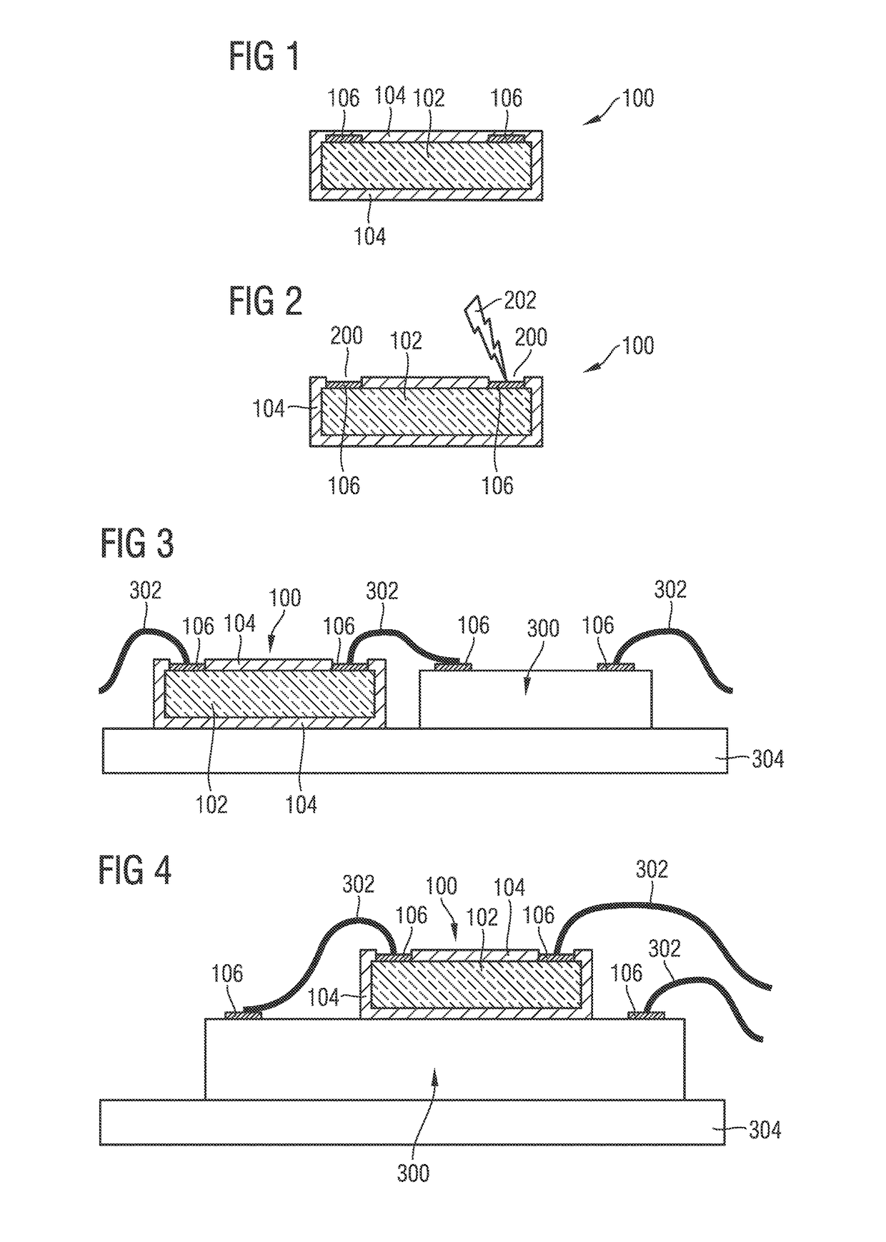
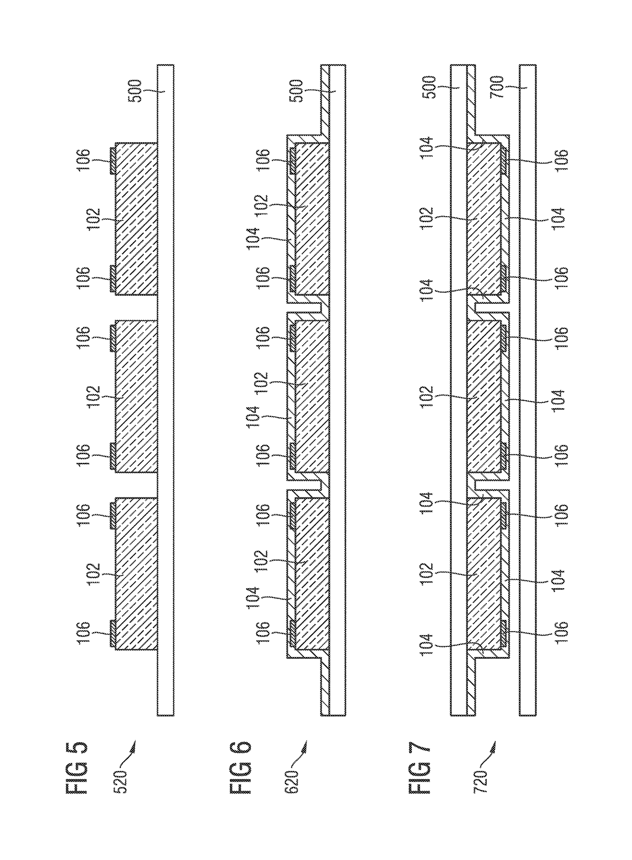
[0017]In the context of the present application, the term “semiconductor chip” may particularly denote a naked die, i.e. a non-packaged (for instance non-molded) chip made of a processed semiconductor, for instance a singulated piece of a semiconductor wafer. One or more integrated circuit elements (such as a diode, a transistor, etc.) may be formed within the semiconductor chip.

[0018]In the context of the present application, the term “pad” may particularly denote an electrically conductive contact or terminal formed on a surface of the naked die which allows to electrically contact the one or more integrated circuit elements of the semiconductor chip. For example, a supply signal, a control signal or a data signal may be conducted from an electronic periphery into an interior of the package and into the semiconductor chip via the one or more pads. In a simila...


PUM


Abstract

An insulated chip comprising a semiconductor chip comprising at least one chip pad and an electrically insulating layer surrounding at least part of the semiconductor chip.

Description

BACKGROUND[0001]Technical Field[0002]Various embodiments relate generally to an insulated chip, packages, and methods of manufacturing packages.[0003]Description of the Related Art[0004]Packages may be denoted as encapsulated electronic chips with electrical connects extending out of the encapsulant and being mounted to an electronic periphery, for instance on a chip carrier such as a printed circuit board.[0005]In particular electronic power packages, for instance half bridge circuits or current sensors, may comprise semiconductor chips which need to be mounted in an electrically insulated manner (in particular with regard to neighbored traces, other chips or other electric potentials in the environment). Conventionally, semiconductor chips are mounted on a mounting base via non-conductive glue body to provide an insulation of at least one metal pad on the semiconductor chip. Also a bulk encapsulant (for instance a mold or a laminate of a dielectric plastic material) may contribute...

Claims


Application Information

Patent Timeline
Patent Type & Authority Patents(United States)
IPC IPC(8): H01L21/00H01L23/00H01L21/78H01L25/065H01L23/522H01L23/31H01L21/56
CPCH01L25/0657H01L21/78H01L23/3114H01L23/3135H01L23/3185H01L23/5226H01L24/19H01L24/20H01L24/96H01L24/97H01L2924/3511H01L2924/15311H01L2924/1461H01L2924/1431H01L2924/1421H01L2924/14H01L2924/10272H01L2924/10253H01L2924/10252H01L2924/1033H01L2924/1032H01L2225/06506H01L2225/0651H01L2224/97H01L21/561H01L21/568H01L25/0655H01L2224/04042H01L2224/04105H01L2224/24137H01L2224/32225H01L2224/32245H01L2224/48091H01L2224/48137H01L2224/48145H01L2224/48227H01L2224/48247H01L2224/73265H01L2224/73267H01L2224/82039H01L2224/92244H01L2924/00H01L2924/00012H01L2224/18
Inventor THEUSS, HORSTBEER, GOTTFRIEDHOEGERL, JUERGEN
Owner INFINEON TECH AG
Why Eureka
Try Eureka