Ring oscillator using current mirror inverter stages

a technology of mirror inverter and oscillator, which is applied in the field of oscillators, can solve the problem of limited maximum value of m and practical considerations

Inactive Publication Date: 2001-04-03
STMICROELECTRONICS SRL
View PDF6 Cites 54 Cited by
  • Summary
  • Abstract
  • Description
  • Claims
  • Application Information

AI Technical Summary

Benefits of technology

The first and second transistors can be n-channel field effect devices having a gate as the control node and the source-drain path as the controllable path. As the transistors are of the same type, process variations affect the transistors in the same manner. The maximum frequency of operation is limited only by the ratio of gain to gate capacitance.

Problems solved by technology

The maximum value of m is limited by practical considerations and particularly layout considerations.

Method used


Image

  • Ring oscillator using current mirror inverter stages
  • Ring oscillator using current mirror inverter stages
  • Ring oscillator using current mirror inverter stages

Examples


Embodiment Construction

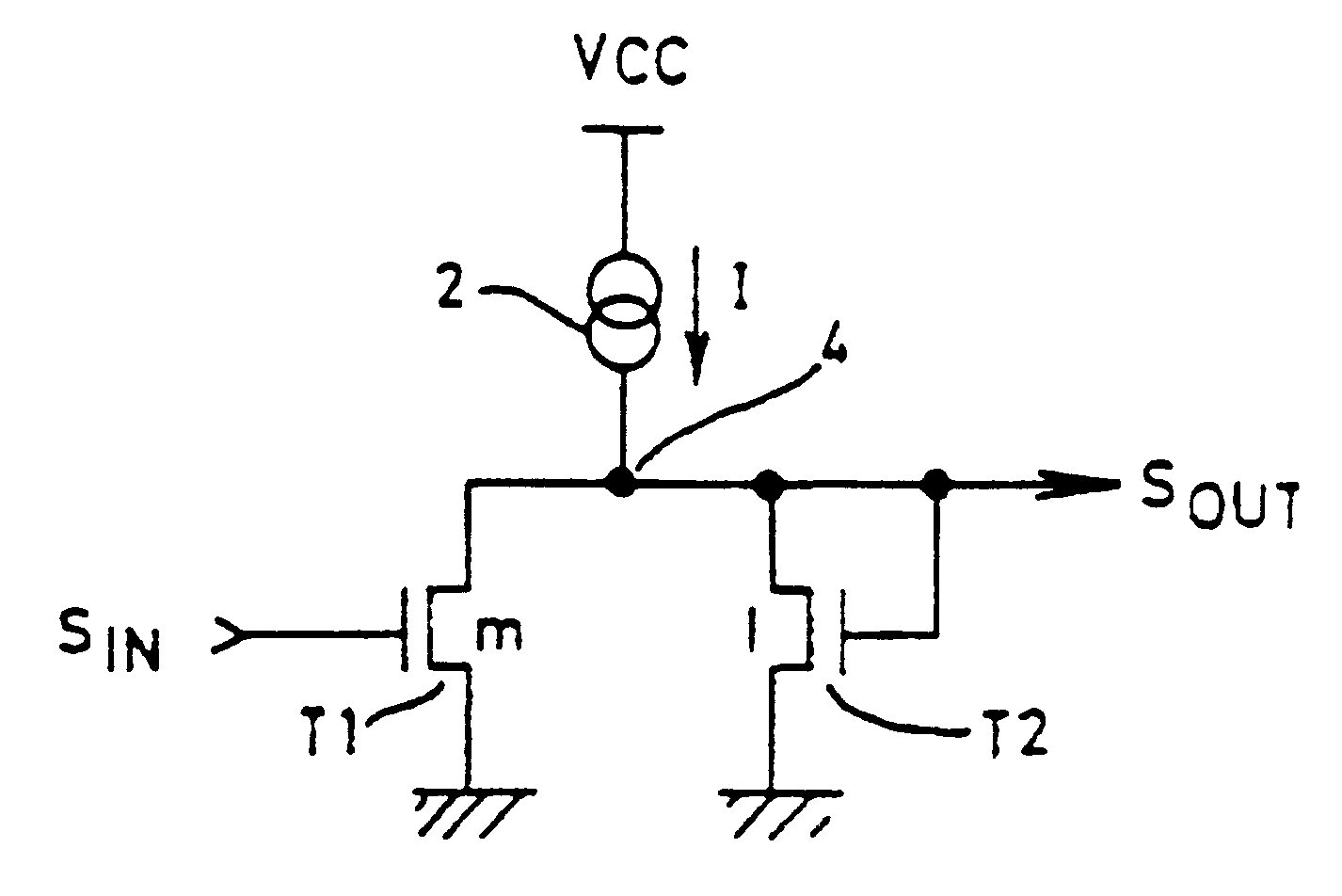
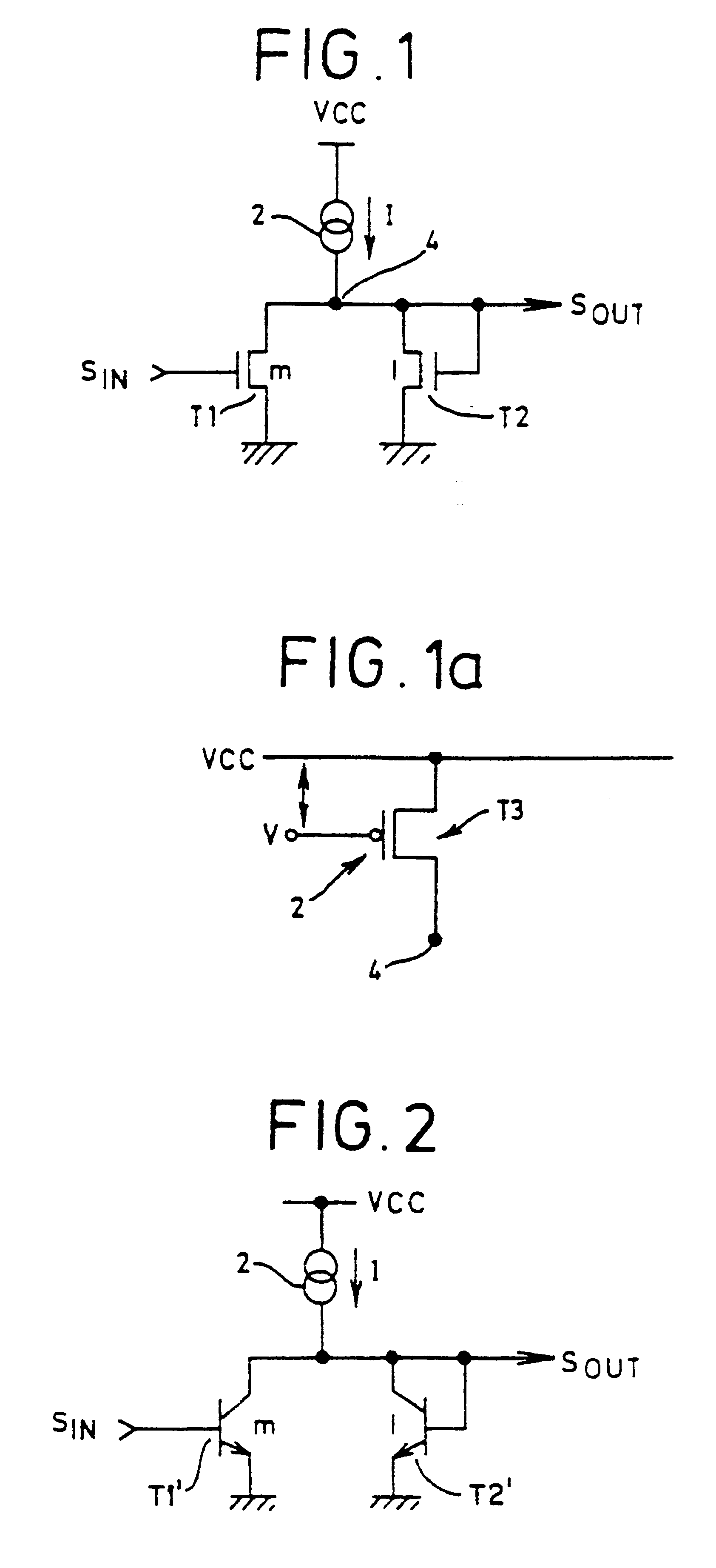
FIG. 1 shows a low-voltage inverting gain stage in MOS technology. The stage comprises first and second transistors T1, T2 which have their drains connected together and their sources connected to ground. The gate of the first transistor T1 acts as the input S.sub.in for the stage and the gate of the second transistor T2 acts as the output S.sub.out. The gate of the second transistor T2 is connected to its drain. Each stage is controlled by a control current I which is generated by a current source 2. The current source 2 is connected between a supply voltage Vcc and the drains of the first and second transistors T1,T2. The common node between the current source 2 and the drains of the transistors T1 and T2 is denoted 4. As shown in FIG. 1a, the current source 2 can comprise a p-channel MOS field effect transistor T3 with its source / drain path connected between the supply voltage Vcc and the node 4 and its gate connected to receive a control signal V which is taken with respect to t...


PUM


Abstract

A ring oscillator having an odd number of single ended stages, each stage including two transistors connected as a current mirror. The stage provides for low-voltage performance and improved process tolerance characteristics.

Description

FIELD OF THE INVENTIONThis invention relates to an oscillator and more particularly to a ring oscillator.BACKGROUND OF THE INVENTIONNew manufacturing processes and new applications are forcing power supplies to lower voltages (3.3 v now, with 2.4 v and 1.5 v being expected soon). Advanced Phase-Locked Loops require stable oscillators which may be varied in frequency by a control signal.To help achieve frequency stability, oscillators integrated into a noisy VLSI environment often use a regulator to generate a quiet power supply. This usually has to be at an even lower voltage than the normal power supply.There is thus a desire to provide oscillators which can work at these very low supply voltages and still produce high quality, high frequency output signals.Reference is made to IBM Technical Disclosure Bulletin, Vol. 31, No. 2, July 1988, pages 154 to 156 "CMOS Ring Oscillator with controlled frequency" which describes a ring oscillator using CMOS transistors and is designed to giv...

Claims


Application Information

Patent Timeline
Patent Type & Authority Patents(United States)
IPC IPC(8): H03K5/13H03K3/00H03K3/03H03K5/00H03K3/282H03K3/0231H03K3/354H03K5/151
CPCH03K3/0231H03K3/03H03K3/0322H03K3/354H03K5/00006H03K5/133H03K5/151H03K2005/00202Y10S331/03
Inventor MONK, TREVOR K.HALL, ANDREW M.
Owner STMICROELECTRONICS SRL
Why Eureka
Try Eureka