Memory device having a relatively wide data bus

a memory device and data bus technology, applied in the field of semiconductor memory, can solve the problems of increasing the cost of forming the dram b>10, limiting the speed of operation of the computer system, and complicating the process

Inactive Publication Date: 2006-01-31
ROUND ROCK RES LLC
View PDF17 Cites 6 Cited by
  • Summary
  • Abstract
  • Description
  • Claims
  • Application Information

AI Technical Summary

Problems solved by technology

Thus, the bandwidth of the system memory is limited by the lower bandwidth of the DRAM, thereby limiting the speed of operation of the computer system.
Alternatively, additional conductive layers could be added to form the additional input / output lines I / O1-I / O4, but this solution complicates the process and increases the cost of forming the DRAM 10.

Method used


Image

  • Memory device having a relatively wide data bus
  • Memory device having a relatively wide data bus
  • Memory device having a relatively wide data bus

Examples


Embodiment Construction

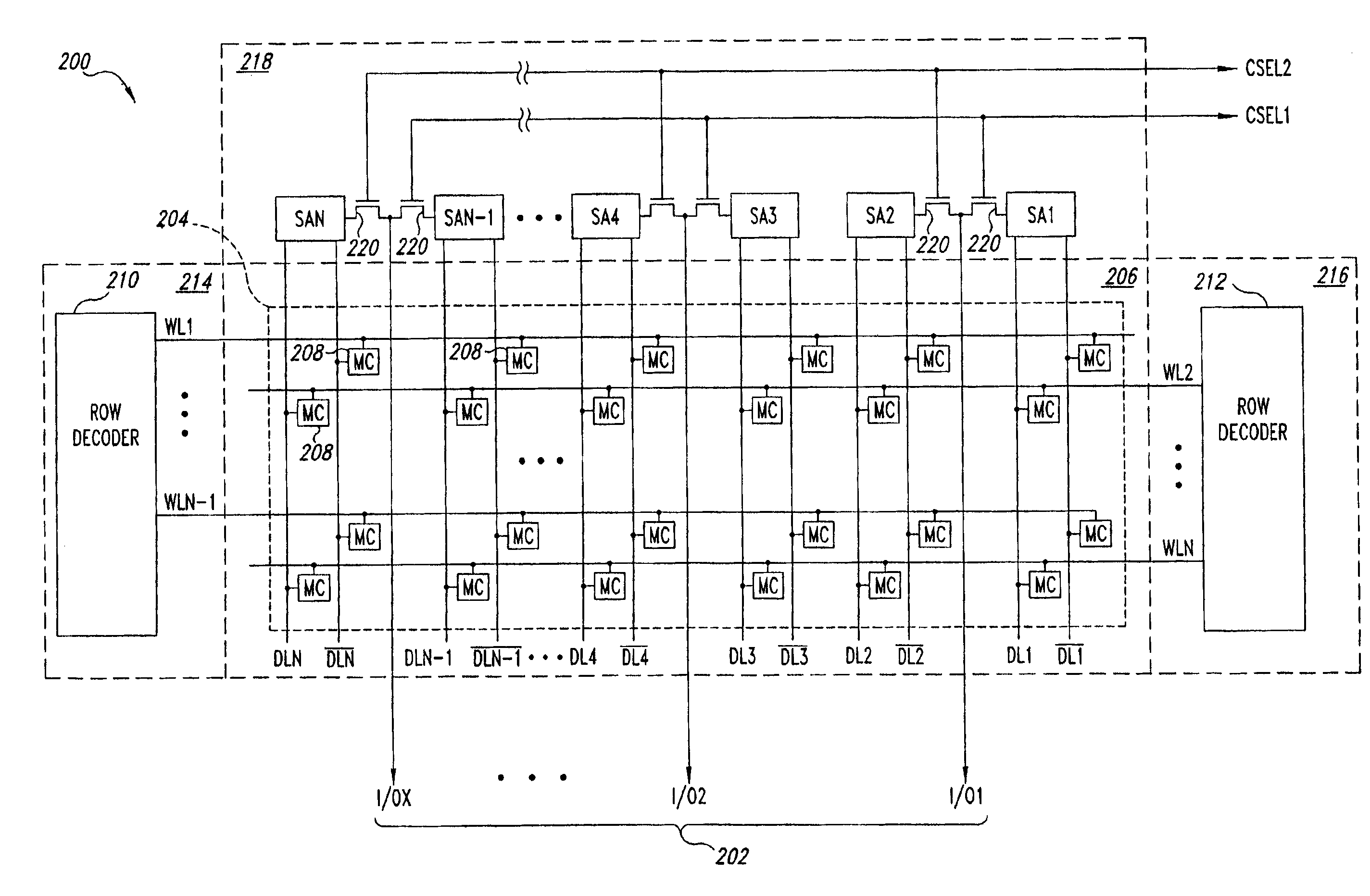
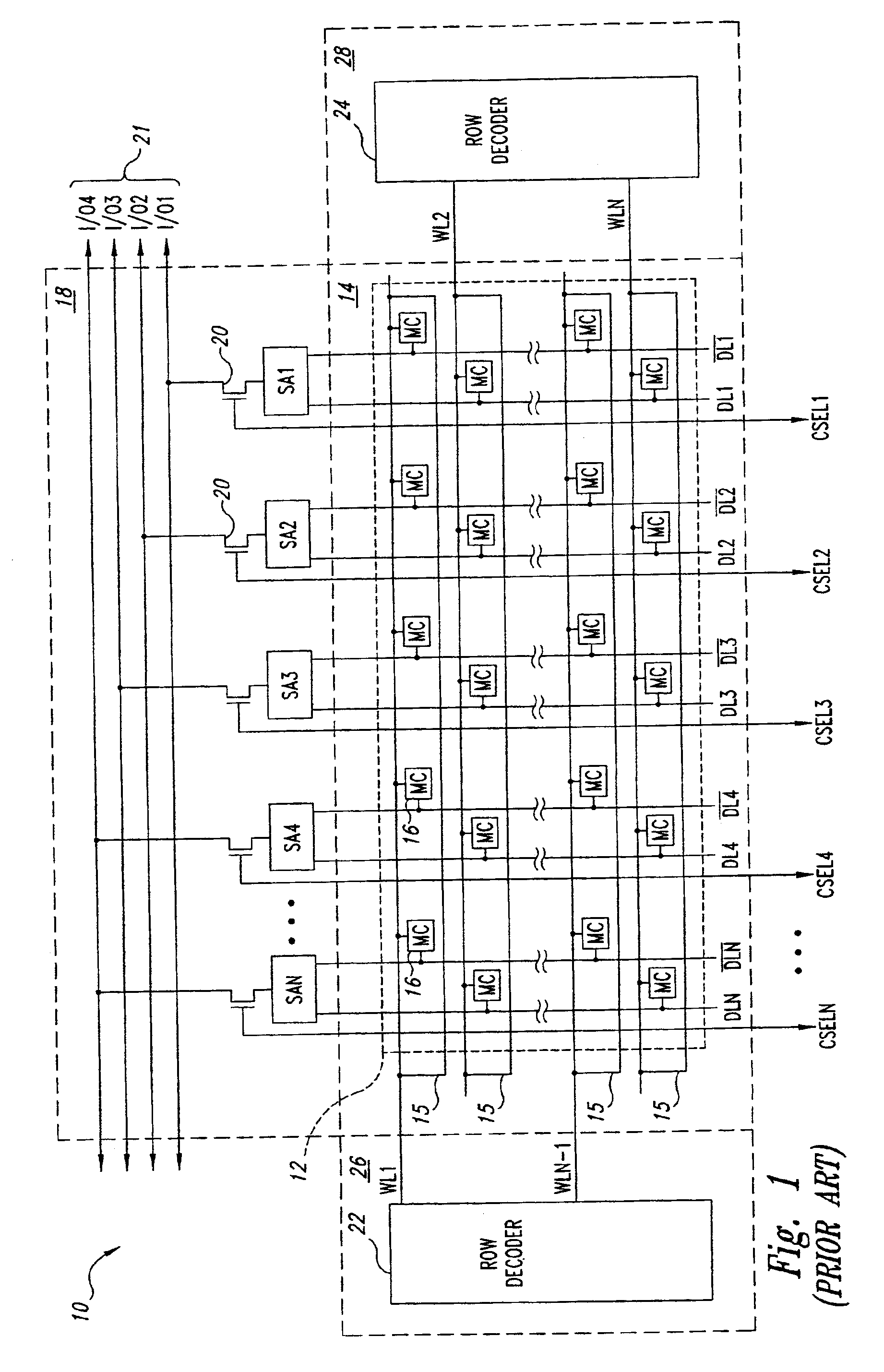
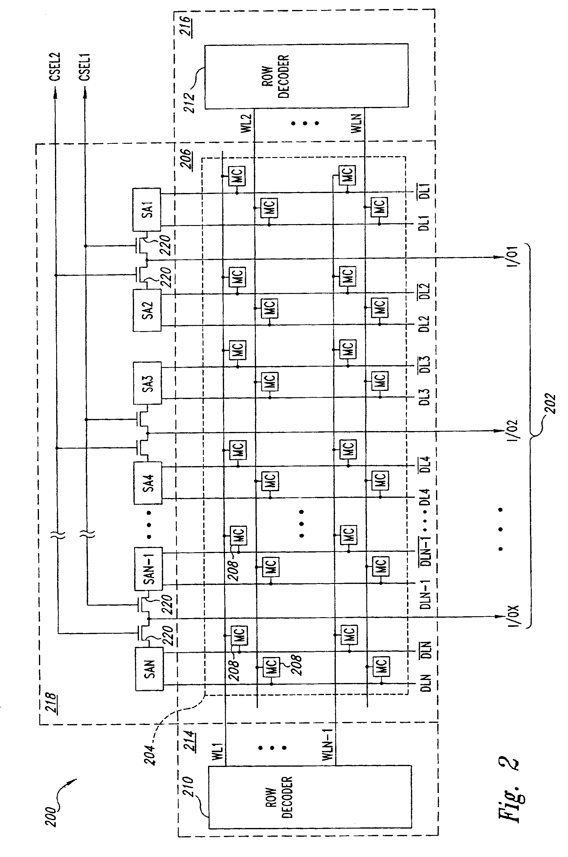
[0019]FIG. 2 is a block diagram of a portion of a DRAM 200 including a wide data path 202 according to one embodiment of the present invention. The wide data path 202 transfers a large block of data accessed in a memory-cell array 204, and may be formed without increasing the size of a semiconductor substrate in which the DRAM 200 is formed, and without requiring the formation of additional conductive layers, as will be explained in more detail below.

[0020]The DRAM 200 includes a memory-cell array 204 formed in an array region 206 of the semiconductor substrate in which the DRAM 200 is formed. The array 204 includes a plurality of memory cells 208 arranged in rows and columns. A plurality of word lines WL1-WLN are formed in a first conductive layer in the array region 206, and are disposed substantially perpendicular to the pairs of digit lines DL1, {overscore (DL1)}-DLN, {overscore (DLN)}. Typically, the first conductive layer is a polysilicon layer formed during fabrication of the...


PUM


Abstract

An architecture for a wide data path in a memory device formed in a semiconductor substrate includes an array of memory cells is formed in an array region of the substrate, the array including a plurality of memory cells arranged in rows and columns. A plurality of complementary pairs of digit lines are formed in the array region from a first conductive layer, each complementary pair being coupled to a plurality of memory cells in an associated column. A plurality of word lines are formed in the array region from a second conductive layer, each word line being coupled to each memory cell in an associated row. A plurality of sense amplifiers are formed in a sense amplifier region of the substrate adjacent the array region, each sense amplifier being coupled to an associated pair of complementary digit lines. A plurality of input / output lines are disposed in a third conductive layer formed above the array region, each input / output line coupled to at least one of the sense amplifiers. At least one column select line is disposed in a portion of the third conductive layer formed above the sense-amplifier region, each column select line being coupled to at least some of the sense amplifiers. The memory device also includes a row address decoder, column address decoder, data path circuit, and control circuit that operate in response to signals applied on respective busses to transfer data to and from the memory device. The architecture may be used, for example, in packetized DRAMs, such as SLDRAMs, and in Embedded DRAMs.

Description

TECHNICAL FIELD[0001]The present invention relates generally to semiconductor memories, and more specifically to a method and architecture for forming internal address decode and data path lines in memory devices having a wide internal data bus.BACKGROUND OF THE INVENTION[0002]In a typical computer system, a microprocessor is coupled to a system memory and executes an application program such as a word processor or a communications program, stored in the memory to perform the desired function of the computer system. To execute the program, the microprocessor accesses instructions and data stored in the system memory. The speed at which the computer system executes the program is determined by the speed of the microprocessor and by the rate at which information is transferred to and from the system memory, which is known as bandwidth of the system memory. Advances in design and fabrication have enabled the processor to operate at increasingly higher speeds, while the speed of the sys...

Claims


Application Information

Patent Timeline
Patent Type & Authority Patents(United States)
IPC IPC(8): G11C7/00G11C7/10G11C11/4096
CPCG11C7/1006G11C7/1048G11C11/4096G11C2207/104
Inventor SHIRLEY, BRIANBUNKER, LAYNE
Owner ROUND ROCK RES LLC
Why Eureka
Try Eureka