Liquid crystal display formed by a plurality of non-electrically interconnected liquid crystal display panels

a liquid crystal display and panel technology, applied in static indicating devices, non-linear optics, instruments, etc., can solve the problems of difficult to see the joints between the liquid crystal panels, and achieve the effects of eliminating the problems, low power consumption, and easy to s

Inactive Publication Date: 2007-11-06
SHARP KK
View PDF17 Cites 1 Cited by
  • Summary
  • Abstract
  • Description
  • Claims
  • Application Information

AI Technical Summary

Benefits of technology

[0023]It is therefore the object of the present invention to present a low-power consuming, high-quality liquid crystal display device that can eliminate the problems caused by the multi-screen display method and make the joints between the liquid crystal panels difficult to see.
[0029]Also, it is desirable that the liquid crystal display further includes a second photo-blocking film which covers the liquid crystal display panels on an end surface of the connected part side along the longitudinal direction in a predetermined trace width. According to this structure, even when the viewer sees a display image diagonally, that is to say, he sees that same through the connected parts of the liquid crystal panels from the external of the liquid crystal display, the second photo-blocking film can curb the light leakage caused by the viewing angle characteristics of the above polarizing elements. Thus, not only a portion where light leaks through the connected parts of the liquid crystal panels shows black under the crossed nicol state of the first and second polarizing elements, but also the light leaking through the area other than the pixel electrodes and the connected parts of the liquid crystal panels can be eliminated in all the directions independently of the viewing angle of the viewer, thereby enabling a natural image on which the joints are more difficult to see.
[0030]In this case, it is desirable that the first photo-blocking film is made of a photo-absorbing film that shows black when having absorbed light. According to this structure, the surface reflection by the first photo-blocking film can be eliminated, thereby making the joints between the liquid crystal panels more difficult to see.
[0034]According to the above structure, unwanted light on an area other than the pixel electrodes can be blocked by the first photo-blocking film, and light passing through the spaces of the connected parts of the liquid crystal panels can be blocked completely by the third photo-blocking film to eliminate the light leakage through the connected parts of the liquid crystal panels completely. Thus, not only the light leakage through the area other than the pixel electrode of each liquid crystal panel 1 but also through the connected parts of the liquid crystal panels can be eliminated completely, thereby enabling a natural image on which the joints are more difficult to see.
[0035]It is desirable that the third photo-blocking film is made of an elastic photo-absorbing material because the irregularity, undulation, stress, etc. on the end surface of the connected parts of the liquid crystal panels can be absorbed by the elasticity of the third photo-blocking film. Since the spaces of the connected parts of the liquid crystal panels can be easily filled by the third photo-blocking film along the shape of the end surface of the connected parts of the liquid crystal panels, the spaces of the connected parts of the liquid crystal panels can be filled completely as a result. Thus, the light leakage through the connected parts of the liquid crystal panels can be eliminated completely, and the joints between the liquid crystal panels are made more difficult to see. Note that to fill the spaces of the connected parts completely with ease, it is desirable to use a photo-absorbing material whose elastic coefficient known as Young's coefficient is 104-108 N / m2, such as a silicon-based rubber, as the elastic photo-absorbing material.

Problems solved by technology

According to the above structure, a portion where light leaks through the connected parts of the liquid crystal panels shows black under the crossed nicol state of the first and second polarizing elements, thereby making the joints between the liquid crystal panels difficult to see.

Method used


Image

  • Liquid crystal display formed by a plurality of non-electrically interconnected liquid crystal display panels
  • Liquid crystal display formed by a plurality of non-electrically interconnected liquid crystal display panels
  • Liquid crystal display formed by a plurality of non-electrically interconnected liquid crystal display panels

Examples


first embodiment

[0055]An embodiment of the present invention will be explained in the following while referring to FIGS. 1 through 4.

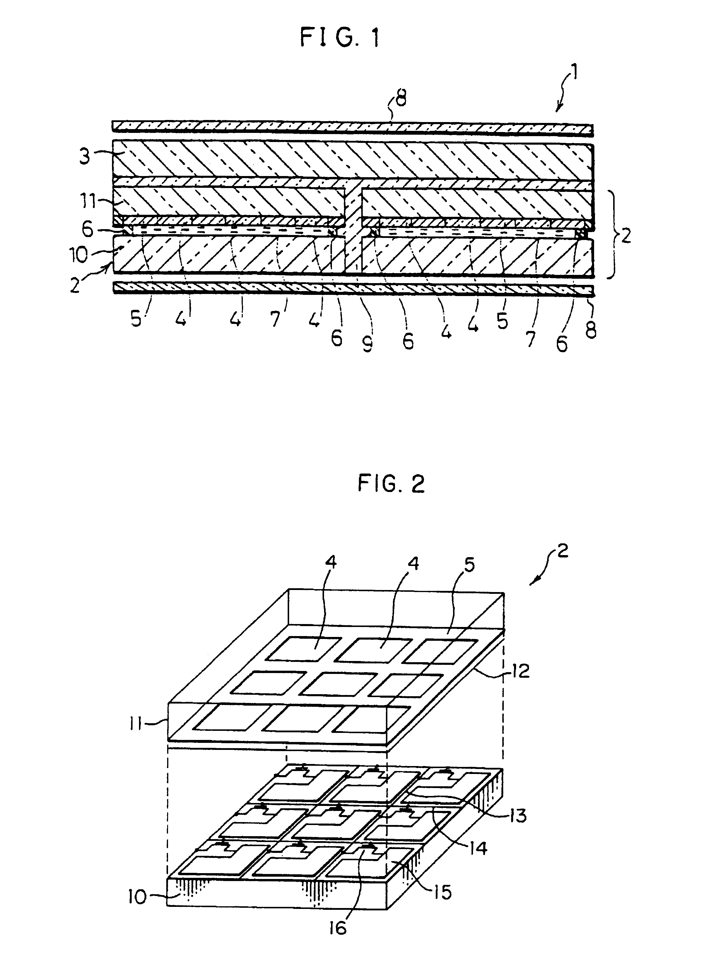
[0056]As shown in FIG. 1, a liquid crystal display 1 of the first embodiment is of the direct sight type. The liquid crystal display 1 comprises a main body and two polarizing plates 8 (polarizing elements). The main body includes a plurality of liquid crystal panels 2 of an active matrix type placed on a single surface of a large substrate 3, and a back light such as a cold cathode tube on the rear surface (lower in the drawing) of the liquid crystal panels 2. The polarizing plates 8 will be described more in detail below. A driver which controls an image signal and the back light are not shown in the drawing. The viewer can see the image data inputted into the liquid crystal panels 2 when the liquid crystal panels 2 modulate the light from the back light in accordance with the input image data.

[0057]As shown in FIG. 2, each liquid crystal panel 2 is of the same stru...

second embodiment

[0089]Another embodiment of the present invention will be explained while referring to FIGS. 1 through 5. Hereinafter, like components are labeled with like numerals with respect to the first embodiment and the description of these components is omitted for the explanation's convenience.

[0090]As shown in FIG. 5, a liquid crystal display 20 of the second embodiment comprises a plurality of liquid crystal panels 2 sandwiched by two large substrate, the large substrate 3 (base) and a large substrate 21 (base). The liquid crystal panels 2 of the second embodiment are of the same structure as those of the first embodiment. The driver controlling the image signal and the back light are not shown in the drawing.

[0091]The liquid crystal display 20 differs from the liquid crystal display 1 of the first embodiment in that the large substrate 21 is additionally laminated to the liquid crystal panels 2 which have already laminated to the single plane of the large substrate 3. The refraction fac...

third embodiment

[0097]Another embodiment of the present invention will be explained while referring to FIGS. 6 through 9. Hereinafter, like components are labeled with like numerals with respect to the above embodiments and the description of these components is omitted for the explanation's convenience.

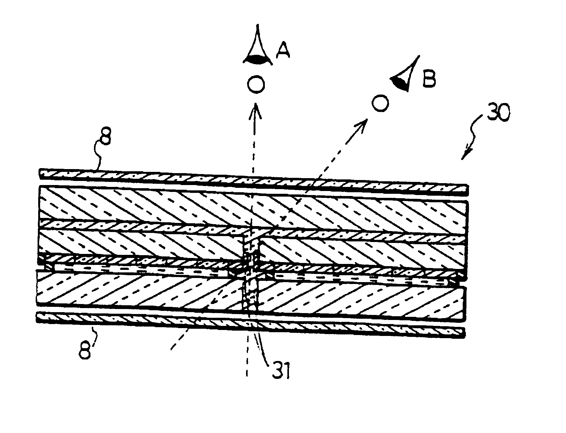
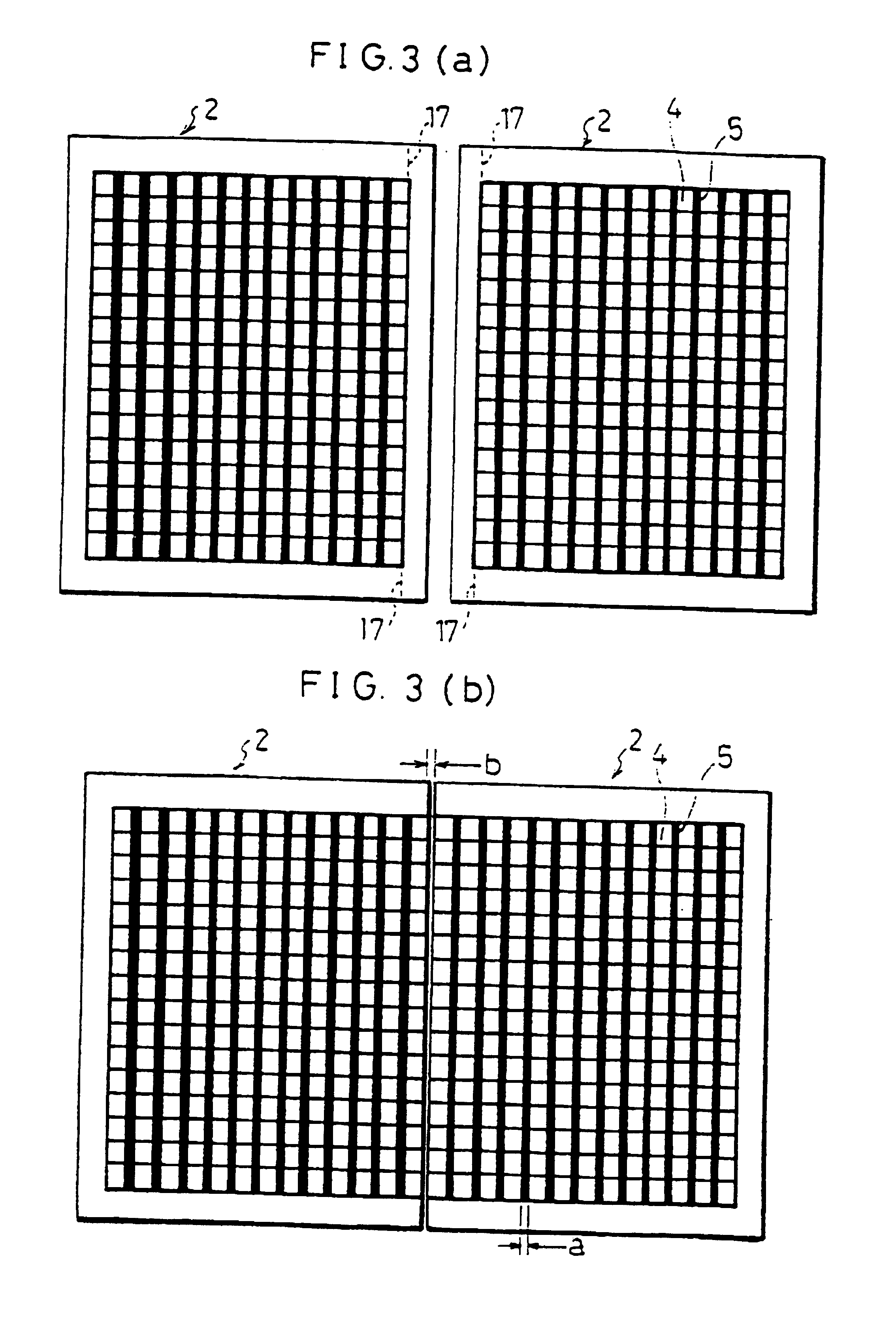
[0098]As shown in FIG. 6, unlike the liquid crystal display 1 of the first embodiment, a liquid crystal display 30 of the third embodiment includes a second photo-blocking films 31 that cover the end surfaces of the connected part side of the liquid crystal panels 2 (the end surface of the glass substrate 11) along a longitudinal direction in a predetermined width. Each second photo-blocking film 31 is perpendicular with respect to the black matrix 5 and extends in a constant width toward the front surfaces of the liquid crystal panels 2. The second photo-blocking films 31 are made of, for example, a black resin made by dispersing a pigment or semi-conducting particulates (for example, carbon partic...


PUM

PropertyMeasurementUnit
thicknessaaaaaaaaaa
thicknessaaaaaaaaaa
thicknessaaaaaaaaaa

Abstract

A liquid crystal display comprising a plurality of liquid crystal panels placed on a single plane of a large substrate, and a black matrix made of a photo-absorbing film that shows black when having absorbed light. Two polarizing plates are respectively placed to cover the front and rear surface of a set of liquid crystal panels almost entirely in such a manner that their polarizing axes intersect at right angles. The resulting multi-screen liquid crystal display consumes less power, retains excellent display quality, and makes the joints between the liquid crystal panels difficult to see.

Description

[0001]This application is a continuation of Pat. No. 08 / 468,649, filed Jun. 6, 1995, abandoned.FIELD OF THE INVENTION[0002]The present invention relates to a liquid crystal display used for AV (audiovisual) systems or OA (office automation) systems.BACKGROUND OF THE INVENTION[0003]Recently, the need for a high-definition large-screen display which is lighter, thinner and less-power-consuming has been increasing for a TV set representing the AV systems intended for home use or the OA systems. For this reason, the development of the large-screen displays including a CRT (cathode ray tube), an LCD (liquid crystal display), a PDP (plasma display panel), an EL (electroluminescent) display, and an LED (light emitting display) has been proceeding toward practical use.[0004]Of all types of displays, the liquid crystal display is most advantageous in that: it has the least depth (thickness); it consumes less power; and it easily displays full color images. Thus, the liquid crystal display ha...

Claims


Application Information

Patent Timeline
Patent Type & Authority Patents(United States)
IPC IPC(8): G02F1/133G02F1/1333G02F1/1339G02F1/1335G02F1/1347
CPCG02F1/13336G02F1/133
Inventor IZUMI, YOSHIHIROFUJIWARA, SAYURISHINOMIYA, TOKIHIKO
Owner SHARP KK
Why Eureka
Try Eureka