
Liquid crystal display device

a liquid crystal display and display device technology, applied in the field of active matrix type liquid crystal display devices, can solve the problems of harmful effect of thermal expansion defective connection between flexible wiring boards, etc., and achieve the effects of preventing waveform distortion of signals, increasing the capacity of interconnection lines of flexible wiring boards, and reducing capacity

Inactive Publication Date: 2009-05-05
PANASONIC LIQUID CRYSTAL DISPLAY CO LTD +1
View PDF15 Cites 7 Cited by
  • Summary
  • Abstract
  • Description
  • Claims
  • Application Information

AI Technical Summary

Benefits of technology

[0014]Moreover, in the trend toward an increase in the size of the liquid crystal display device constructed in the above-described manner, it has been pointed out that a waveform distortion easily occurs in a video signal which is transmitted through a video signal line or lines located on one side in the direction of juxtaposition of video signal lines among a plurality of video signal lines juxtaposed over the main surface of the substrate.
[0028]Accordingly, in spite of an increase in the size of the liquid crystal display panel, it is possible to prevent waveform distortion from occurring in a signal on a signal line which lies on one side of the liquid crystal display panel in the direction of juxtaposition of the signal lines.

Problems solved by technology

However, in a trend toward an increase in the size of the liquid crystal display device constructed in the above-described manner, it has been pointed out that a defective connection occasionally occurs between the flexible wiring board and one transparent substrate of the liquid crystal display panel.
It has also been found out that the harmful effect of thermal expansion of the flexible wiring board occurs not only while the flexible wiring board is being connected to one of the transparent substrates of the liquid crystal display panel, but also after the flexible wiring board has been connected.

Method used


Image

  • Liquid crystal display device
  • Liquid crystal display device
  • Liquid crystal display device

Examples


embodiment 1

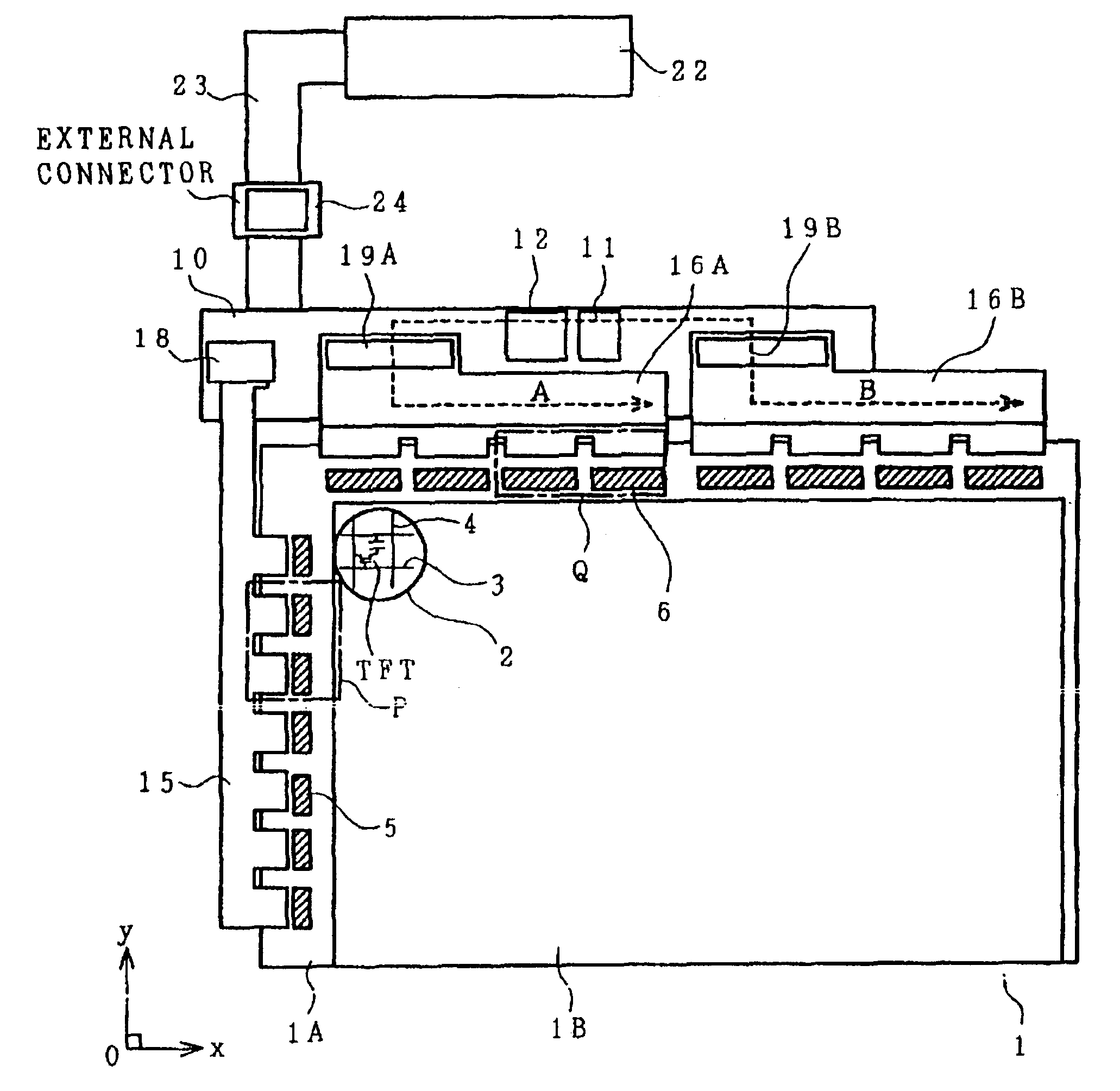
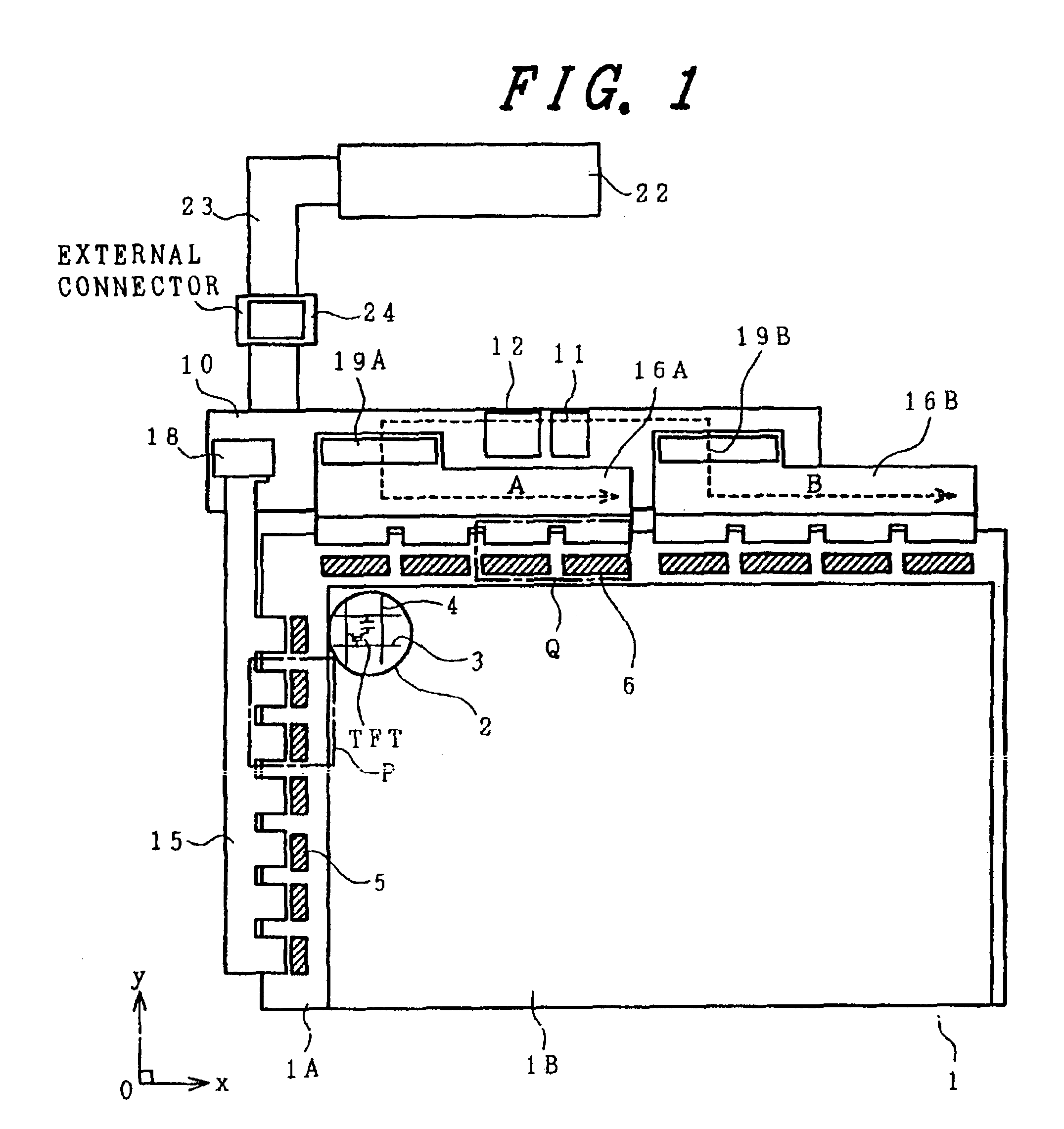
[0042]FIG. 1 is a schematic view showing, the structure of the entire liquid crystal display device according to the present invention.

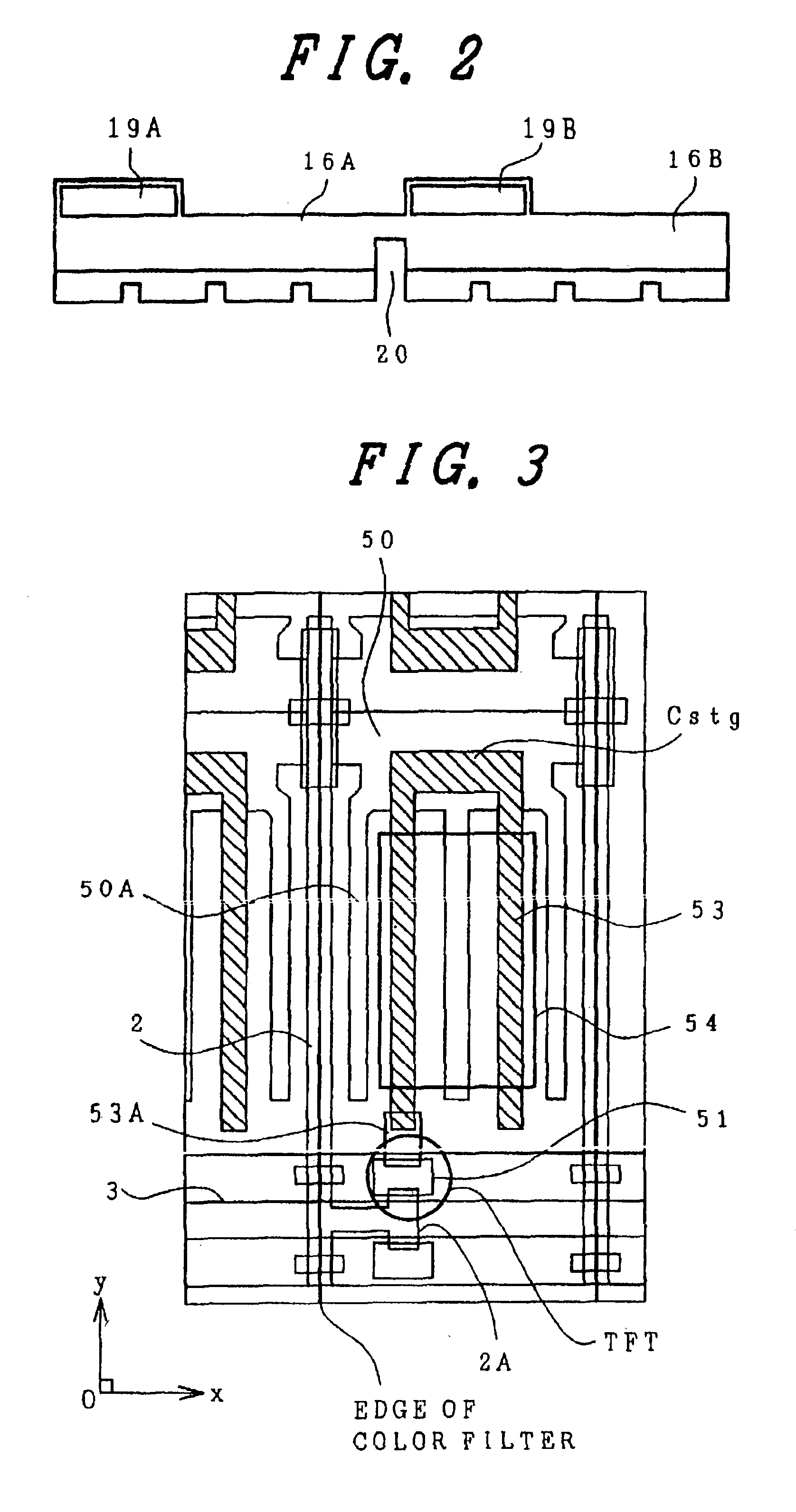
[0043]In this embodiment, the present invention is applied to a liquid crystal display device which adopts a so-called lateral electric field type (also called an In-Plane-Switching type or IPS type) known as a type having a wide viewing angle.

[0044]In FIG. 1, a liquid crystal display panel 1 is constructed as a chamber for a liquid crystal (not shown) which has transparent substrates 1A and 1B arranged to oppose each other across the liquid crystal. In this case, one of the transparent substrate (the lower substrate shown in FIG. 1: the matrix substrate 1A) is formed to be slightly larger than the other transparent substrate (the upper substrate shown in FIG. 1: the color filter substrate 1B), and, as viewed in FIG. 1, the bottom and right edges of the transparent substrate 1A are nearly flush with the bottom and right edges of the transparent subst...


PUM

PropertyMeasurementUnit
stressaaaaaaaaaa
transparentaaaaaaaaaa
optical transmissivityaaaaaaaaaa

Abstract

In spite of an increase in the size of a liquid crystal display panel, it is possible to prevent the defective connection of a flexible wiring board to a transparent substrate of the liquid crystal display panel. A liquid crystal display device includes a pair of transparent substrates arranged to oppose each other across a liquid crystal, for which they are utilized to form a chamber, a plurality of pixels formed along a spreading direction of the liquid crystal, driving circuits for supplying video signals to the pixels, and a flexible wiring board for supplying signals to the input sides of the driving circuits from a substrate on which a control circuit is mounted, the flexible wiring board being divided into a plurality of portions.

Description

BACKGROUND OF THE INVENTION[0001]1. Field of the Invention[0002]The present invention relates to a liquid crystal display device and, more particularly, to an active matrix type of liquid crystal display device.[0003]2. Description of the Related Art[0004]An active matrix type of liquid crystal display device is characterized by a structure in which a switching element made of, for example, a thin-film transistor (TFT) is incorporated in each pixel of its liquid crystal display panel.[0005]The active matrix type of liquid crystal display device has, as a chamber for a liquid crystal, a pair of substrates (at least one of which is a so-called transparent substrate having a sufficient optical transmissivity) which are arranged to oppose each other across the liquid crystal, and a pixel group is formed in a direction in which the liquid crystal is spread along the main surface of this substrate. This pixel group includes pixels each of which is provided in a portion surrounded by two a...

Claims


Application Information

Patent Timeline
Patent Type & Authority Patents(United States)
IPC IPC(8): G02F1/1345G09G3/36G09G5/00G02F1/13G02F1/133
CPCG02F1/13452G02F1/133
Inventor MISHIMA, YASUYUKIMORISHITA, SHUNSUKE
Owner PANASONIC LIQUID CRYSTAL DISPLAY CO LTD
Learn More