Supercharge Your Innovation With Domain-Expert AI Agents!

Method for controlling a non-volatile semiconductor memory device

a non-volatile semiconductor and memory device technology, applied in the direction of static storage, digital storage, instruments, etc., can solve the problems of interference noise, becoming more difficult to avoid interference noise between adjacent cells, and noise interferen

Active Publication Date: 2018-03-06
K K PANGEA
View PDF37 Cites 3 Cited by
  • Summary
  • Abstract
  • Description
  • Claims
  • Application Information

AI Technical Summary

Benefits of technology

The proposed method effectively reduces back pattern noise and threshold voltage shifts, improving data integrity and storage accuracy in highly integrated NAND-type flash memories by carefully managing the read pass voltages applied to unselected memory cells, particularly in designs with smaller feature sizes.

Problems solved by technology

What becomes problematic whenProblems occur as the NAND-type flash memory is more highly integrated and stores more data bits per cell is; creating an interference noise between floating gates.
However, as the highlyhigher integration of the NAND-type flash memories progresses, there is possibility that it becomes more difficult to avoid the interference noise between adjacent cells.

Method used


Image

  • Method for controlling a non-volatile semiconductor memory device
  • Method for controlling a non-volatile semiconductor memory device
  • Method for controlling a non-volatile semiconductor memory device

Examples


Embodiment Construction

[0040]Illustrative embodiments of this invention will be explained with reference to the accompanying drawings below.

[0041]Basic Configuration and Basic Write-control Scheme

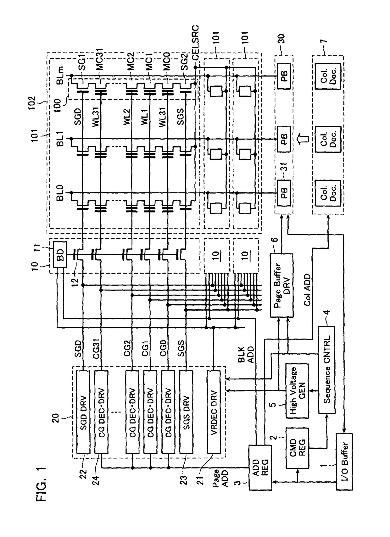
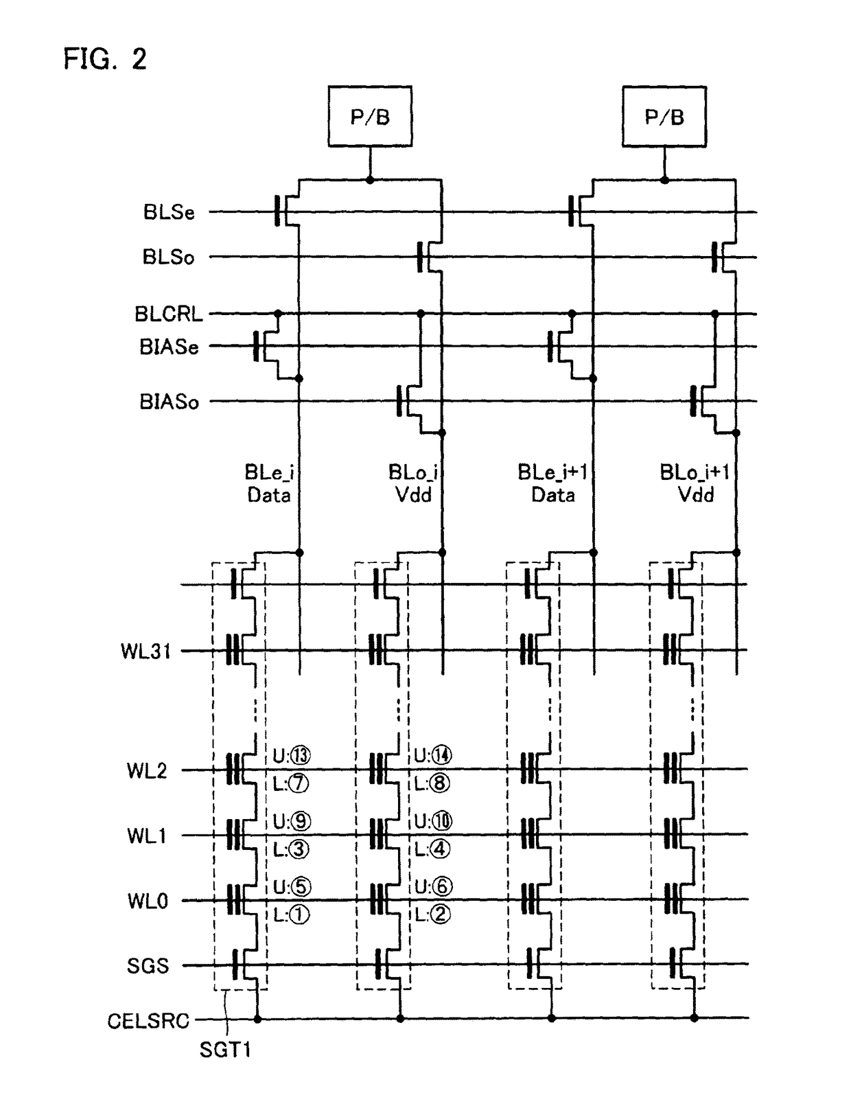
[0042]FIG. 1 shows the whole configuration of a NAND-type flash memory in accordance with an embodiment. NAND cell unit (i.e., NAND string) 100, which is a basic unit of the NAND-type flash memory, has plural memory cells MC0-MC31 connected in series and two select gate transistors SG1 and SG2 disposed at the both ends.

[0043]One end of NAND cell unit 100 is coupled to bit line BL via the select gate transistor SG1; and the other end is coupled to common source line CELSRC via the select gate transistor SG2.

[0044]One memory cell has N-type source and drain diffusion layers formed on a P-well formed on a silicon substrate, and a stacked gate structure with a floating gate and a control gate stacked above the channel region defined by the source and drain layers. ChangingBy changing the charge amount held in the flo...


PUM


Abstract

A non-volatile semiconductor memory device has a NAND string, in which multiple memory cells are connected in series. A read procedure is performed for a selected memory cell in the NAND string on the condition that the selected memory cell is applied with a selected voltage while unselected memory cells are driven to be turned on without regard to cell data thereof. In the read procedure, a first read pass voltage is applied to unselected memory cells except an adjacent and unselected memory cell disposed adjacent to the selected memory cell, the adjacent and unselected memory cell being completed in data write later than the selected memory cell, and a second read pass voltage higher than the first read pass voltage is applied to the adjacent and unselected memory cell.

Description

CROSS-REFERENCE TO RELATED APPLICATION[0001]This application is based on and claims the benefit of priority from the prior Japanese Patent Application No. 2007-239089, filed on Sep. 14, 2007, the entire contents of which are incorporated herein by reference.BACKGROUND OF THE INVENTION[0002]1. Field of the Invention[0003]This invention relates to a non-volatile semiconductor memory device with a floating gate type memory cell of a floating gate type, and specifically relates to a method of controlling read / write of a NAND-type flash memory.[0004]2. Description of the Related Art[0005]A currently manufactured NAND-type flash memory has floating gate type of memory cells, wherein write and erase of whichoperations are performed with electron-injection and electron-releasing ofat the respective floating gates (FGs). ControllingBy controlling the electron injection quantity in a floating gate, it is ablepossible to set multiple threshold voltage states (i.e., data states). In practice, i...

Claims


Application Information

Patent Timeline
Patent Type & Authority Patents(United States)
IPC IPC(8): G11C16/06G11C11/56G11C16/04G11C16/26G11C16/34
CPCG11C11/5642G11C16/0483G11C16/26G11C16/3418G11C16/3454G11C2211/565G11C16/34G11C16/02
Inventor HOSONO, KOJI
Owner K K PANGEA
Features
  • R&D
  • Intellectual Property
  • Life Sciences
  • Materials
  • Tech Scout
  • Unparalleled Data Quality
  • Higher Quality Content
  • 60% Fewer Hallucinations
Learn More