Method for automatic generating device mark in printed circuit board design

A technology for automatically generating and printing circuit boards, which is applied in the fields of printed circuits, printed circuit manufacturing, and electrical components. The font is consistent and the effect of improving design efficiency

Inactive Publication Date: 2007-10-03
WUS PRINTED CIRCUIT (KUNSHAN) CO LTD
View PDF4 Cites 1 Cited by
  • Summary
  • Abstract
  • Description
  • Claims
  • Application Information

AI Technical Summary

Problems solved by technology

[0004] Due to the large number of device marks that need to be adjusted and placed, it is easy to cause fatigue to the designer; it is very easy to make mistakes such as misalignment of device marks, which directly affects production, processing, development and debugging; the workload is heavy, which is the bottleneck for improving design efficiency

Method used


Image

  • Method for automatic generating device mark in printed circuit board design
  • Method for automatic generating device mark in printed circuit board design
  • Method for automatic generating device mark in printed circuit board design

Examples


Embodiment Construction

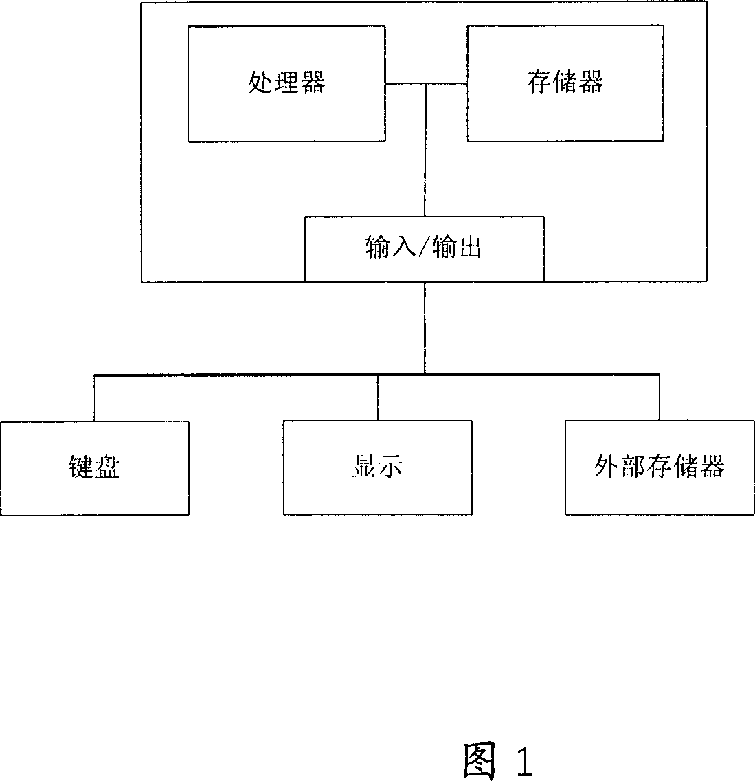
[0026] Figure 1 shows a computer used to implement the invention. The computer has a processor, which is connected to the memory through the bus, and is also connected to the input and output interfaces through the bus. The memory stores the circuit printed board design program. The input and output interface is connected to the keyboard, external memory and display, and the circuit printed board diagram is displayed through the display, or output through an output device such as a printer connected to the computer.

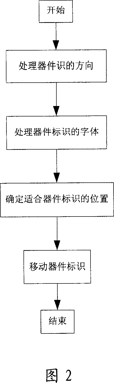
[0027] Since the device identification in the circuit printed board diagram generated by the computer device needs to meet the requirements from the process, production, debugging, specification, etc., after abstract processing, these requirements are transformed into the printed circuit board (referred to as PCB) design. Finally, it is required that the placement position of the device logo can be in the customary position that is usually manually adjusted. The...


PUM


Abstract

The method is as the follows: character string information used for device identification is fetched from information bank stored with circuit board drawing and treatment is carried out to attribute of character string to satisfy ruled identification direction and character style, an identification regional series (IRS) formed by multiple subregion of candidate identification (CI) is confirmed around device according to distance value of appointed device identification to corresponding device and a CI subregion suitable to place device identification is confirmed from the IRS according to avoidane of priority control as well as device identification is generated at the identification subregion.

Description

technical field [0001] The invention relates to a method for automatically generating device identification in printed circuit board design. Background technique [0002] After the design of the printed circuit board (referred to as PCB) is completed, it is necessary to place the device identification of all devices in the PCB design in a suitable position. Usually, the number of components in PCB design is quite large, and whether the position and direction of the component identification is correct or not directly affects the subsequent production, processing, development and debugging, so this work is also of considerable importance. The existing technology for placing the component marks on the PCB is completely done manually by the designer without any auxiliary tools to help. [0003] There is following shortcoming in prior art: [0004] Due to the large number of device marks that need to be adjusted and placed, it is easy to cause fatigue to the designer; it is ver...

Claims


Application Information

Patent Timeline
Patent Type & Authority Patents(China)
IPC IPC(8): H05K3/00G06F17/50
Inventor 景丰华
Owner WUS PRINTED CIRCUIT (KUNSHAN) CO LTD
Why Eureka
Try Eureka