Address multiplexing logic implementation method with SDRAM compatible

A technology of address multiplexing and logic, which is applied in the field of compatibility between address multiplexing logic and SDRAM, and achieves the effects of simple software operation, convenient logic implementation, and fewer control signals

Inactive Publication Date: 2007-10-17
HUAWEI TECH CO LTD
View PDF4 Cites 0 Cited by
  • Summary
  • Abstract
  • Description
  • Claims
  • Application Information

AI Technical Summary

Problems solved by technology

[0008] Comparing the above two driving methods, it is found that although the column address of the latter is only increased by one bit, the information of each bit of the linear address of the processor has changed greatly as a result. Therefore, it is necessary to make the same printed circuit board (PCB) design. Compatible with SDRAMs of different capacities, the multiplexing method of the address multiplexing logic unit must be able to be flexibly modified through software settings

Method used


Image

  • Address multiplexing logic implementation method with SDRAM compatible
  • Address multiplexing logic implementation method with SDRAM compatible
  • Address multiplexing logic implementation method with SDRAM compatible

Examples


Embodiment Construction

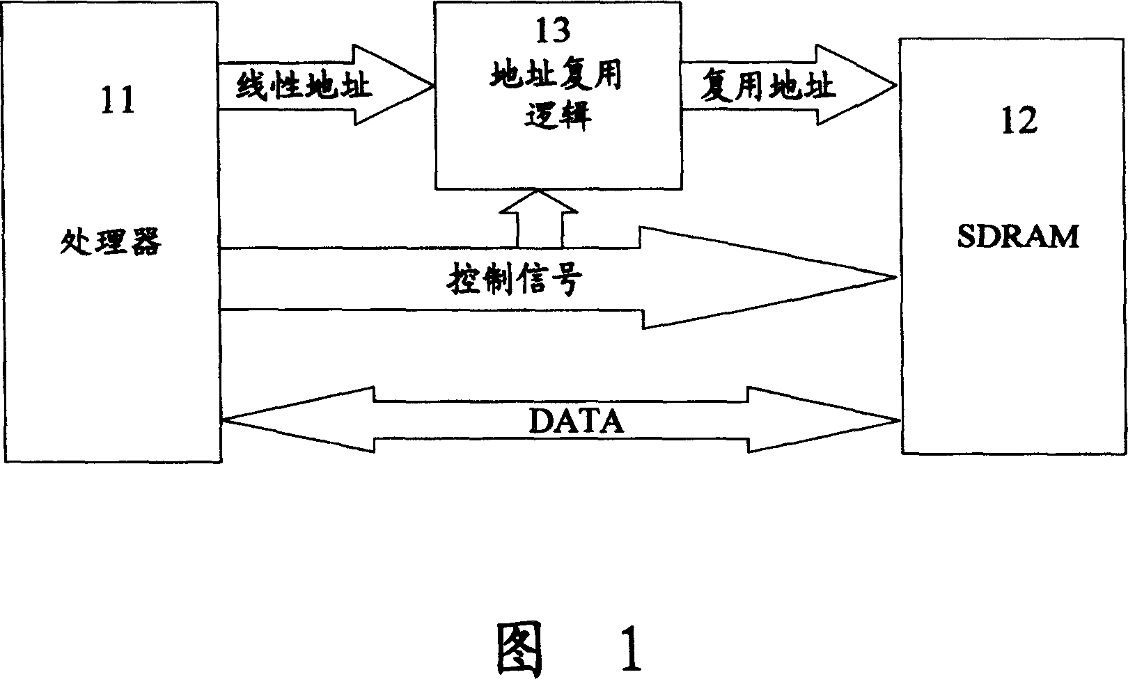
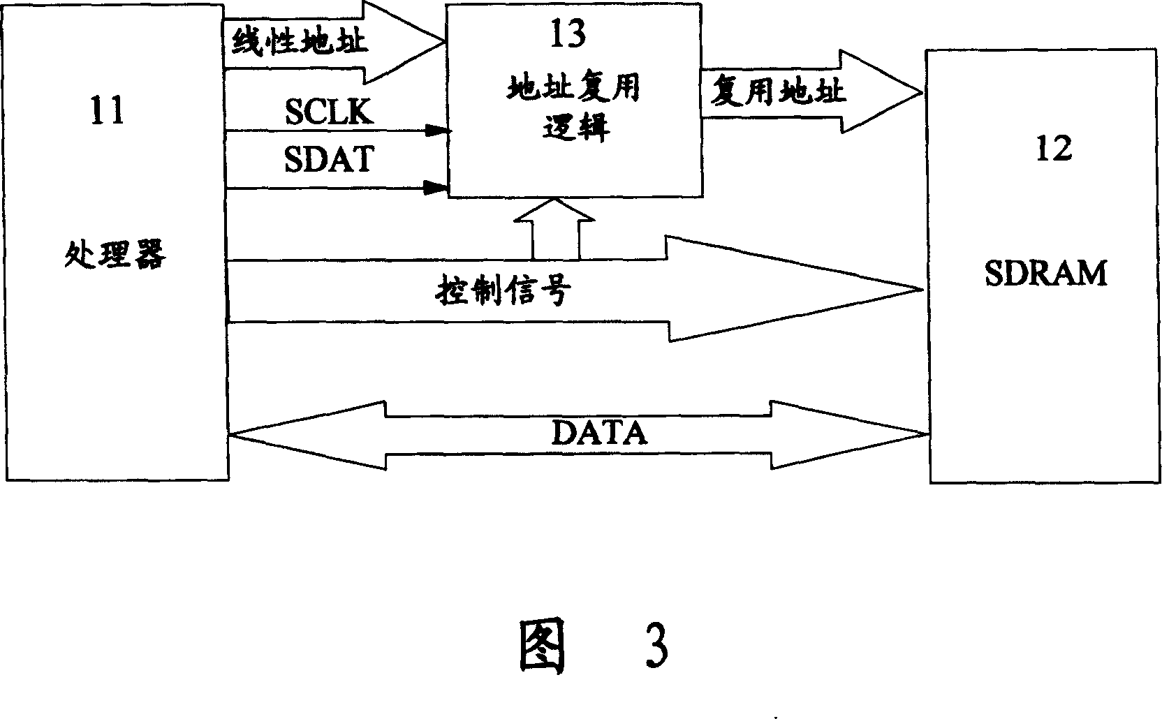
[0028] The object of the present invention is realized by adding an interface between the address multiplexing logic unit and the processor, including a clock signal line (SCLK) and a data signal line (SDAT).

[0029] Processor I / O

foot name

signal direction

Functional description

Defaults

SCLK

Processor --> Address Multiplexing

logic unit

Clock line, address multiplexing logic unit sampling reception

The clock SCLK required for SDAT, the clock passes through

The SCLK line is sent to the address multiplexing logic unit

high level

SDAT

Processor --> Address Multiplexing

logic unit

data line, used to send SDRAM driver information, the

Driver information is sent by the processor via the SDAT line to the

Address multiplexing logic unit;

Processor on the falling edge (or rising edge) of SCLK

To send SDAT data, the address multiplexing lo...


PUM


Abstract

The invention relates to a method of implementing the compatibility of address multiplexing logic with SDRAM by, using a processor to send control word to the address multiplexing logic so as to make the address multiplexing compatible with the SDRAMs of various driving modes, and it includes: the processor selects the sequence code of control word according to the driving mode of SDRAM, and the selected sequence code corresponds to the current driving mode of SDRAM; under the synchronous control of a clock signal, the processor writes the sequence code in address multiplexing logic unit; the logic unit judges if the received sequence code matches with the desired value of sequence code: if it does, select the corresponding driving mode of SDRAM to the desired value and make line and column address multiplexing processing on the linear address outputted by the processor; otherwise, keep the original driving mode of SDRAM, such as a default driving mode. Both the clock signal and sequence code signal are led through a universal pin on the processor to the address multiplexing logic unit. It can be applied in any circumference of using processors and memories.

Description

technical field [0001] The present invention relates to an application technology of SDRAM, more precisely, it relates to the technology of realizing compatibility between address multiplexing logic and SDRAM, which can be applied to any occasion using processor and memory, such as communication, computer, artificial intelligence, instrumentation, etc. . Background technique [0002] In some cases, the address sent by the SDRAM controller of the processor is a linear address, but the address required by SDRAM and memory sticks using SDRAM is a row and column multiplexed address. In order for the processor to access SDRAM, it must An address multiplexing logic is added between the processor and SDRAM. This address multiplexing logic performs row and column multiplexing on the linear address sent by the processor, and then sends the multiplexed row and column addresses to SDRAM or SDRAM memory. The connection relationship between the processor and SDRAM is shown in Figure 1. ...

Claims


Application Information

Patent Timeline
Patent Type & Authority Patents(China)
IPC IPC(8): G06F12/00G06F1/04
Inventor 李友谊方卫峰牛从亮马全红
Owner HUAWEI TECH CO LTD
Why Eureka
Try Eureka