Film semiconductor device, its manufacturing method, electro-optical device, and electronic apparatus
A technology of thin film semiconductor and manufacturing method, which is applied in the field of manufacturing of electronic machines and capacitive elements, and can solve problems such as low efficiency
- Summary
- Abstract
- Description
- Claims
- Application Information
AI Technical Summary
Problems solved by technology
Method used
Image


Examples
Embodiment approach 1
[0034] (Overall configuration of liquid crystal device)
[0035] figure 1 (A) and (B) are plan views of the liquid crystal device and components formed thereon viewed from the side of the counter substrate, and a plan view including the counter substrate, respectively. figure 1 (A) H-H' sectional view.
[0036] exist figure 1In (A) and (B), in the liquid crystal device 100 (electro-optical device), the TFT array substrate 10 (thin film semiconductor device) and the opposing substrate 20 are coated with a sealing material 107 along the edge of the opposing substrate 20 ( figure 1 (A) The slashed area in the lower right) fit. Furthermore, liquid crystal 50 as an electro-optic substance is held between the TFT array substrate 10 and the counter substrate 20 . On the outer peripheral side of the TFT array substrate 10, a data line driving circuit 101 is formed to partially overlap the sealing material 107 on the side of the substrate side 111, and a scanning line driving circu...
Embodiment approach 2
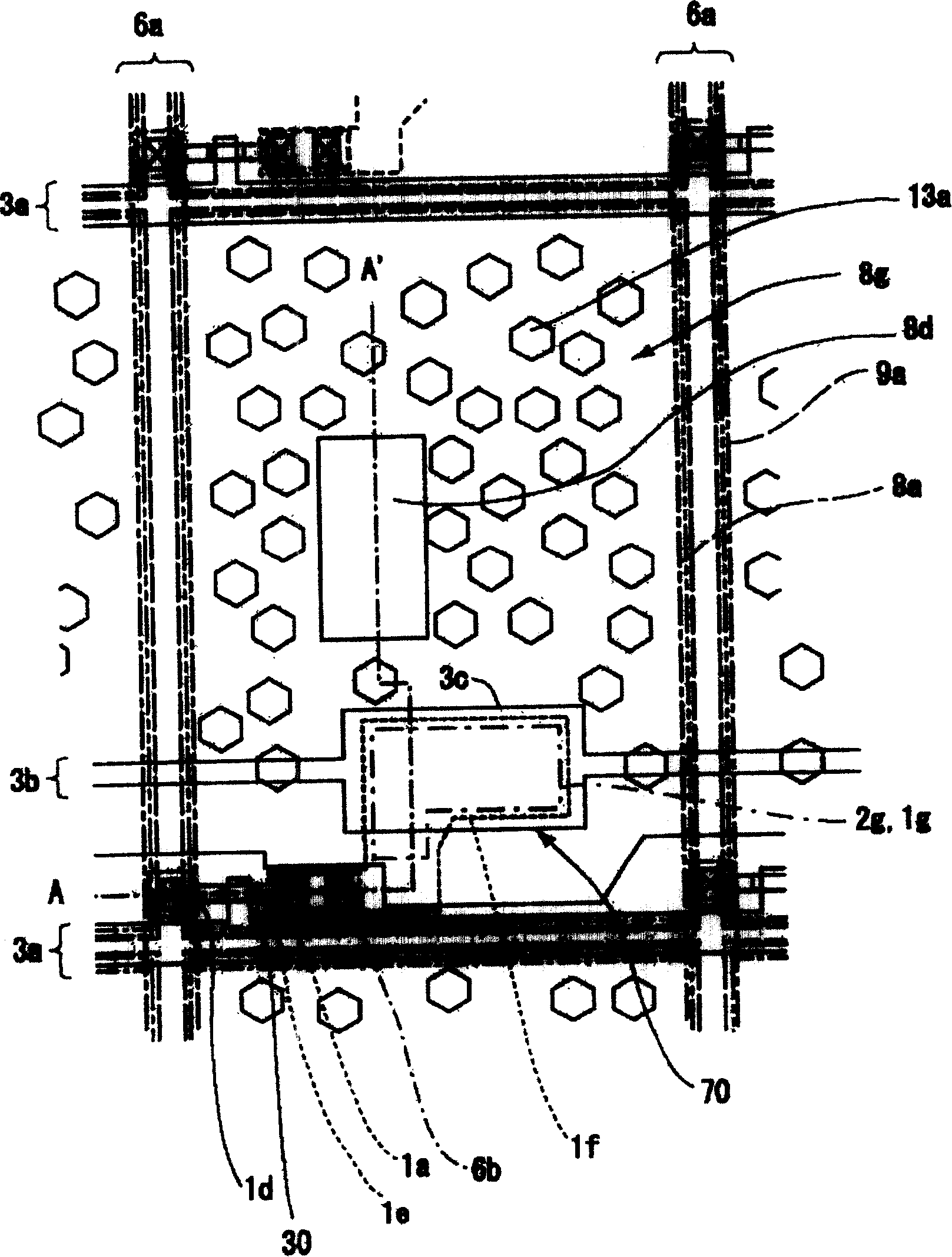
[0074] (Structure of TFT array substrate)
[0075] Figure 8 represents the TFT array substrate of the electro-optical device according to Embodiment 2 of the present invention, and is equivalent to image 3 An explanatory diagram of the cross-section at the position of the A-A' line. Figure 9 It is a cross-sectional view showing the structure of TFTs constituting peripheral circuits such as a scanning line driving circuit and a data line driving circuit in the TFT array substrate of the electro-optical device according to the present embodiment. In addition, since the basic configuration of the electro-optical device of this embodiment is the same as that of Embodiment 1, common parts are given the same reference numerals and their descriptions are omitted.
[0076] Such as Figure 8 As shown, in the present embodiment, also in the storage capacitor 70, the recessed portion 2g (first recessed portion) having the film thickness of the dielectric film 2c thinner than the fi...
PUM
| Property | Measurement | Unit |
|---|---|---|
| thickness | aaaaa | aaaaa |
Abstract
Description
Claims
Application Information
 - R&D
- Intellectual Property
- Life Sciences
- Materials
- Tech Scout
- Unparalleled Data Quality
- Higher Quality Content
- 60% Fewer Hallucinations
Browse by: Latest US Patents, China's latest patents, Technical Efficacy Thesaurus, Application Domain, Technology Topic, Popular Technical Reports.
© 2025 PatSnap. All rights reserved.Legal|Privacy policy|Modern Slavery Act Transparency Statement|Sitemap|About US| Contact US: help@patsnap.com