An assembly, a lithographic apparatus, and a device manufacturing method

A lithography and component technology, which is used in semiconductor/solid-state device manufacturing, photolithography process exposure devices, microlithography exposure equipment, etc., can solve the problems of increasing the complexity of projection optical components and high cost of spacers

Inactive Publication Date: 2009-02-11
ASML NETHERLANDS BV
View PDF8 Cites 0 Cited by
  • Summary
  • Abstract
  • Description
  • Claims
  • Application Information

AI Technical Summary

Problems solved by technology

One problem is that the use of spacers is expensive, especially in terms of sizing, the labor required to grind the spacers to size, and mount the spacers to the support frame
Furthermore, the large number of components increases the complexity of the resulting projection optics assembly, which leads to long-term stability issues related to positioning the elements relative to each other

Method used


Image

  • An assembly, a lithographic apparatus, and a device manufacturing method
  • An assembly, a lithographic apparatus, and a device manufacturing method
  • An assembly, a lithographic apparatus, and a device manufacturing method

Examples


Embodiment Construction

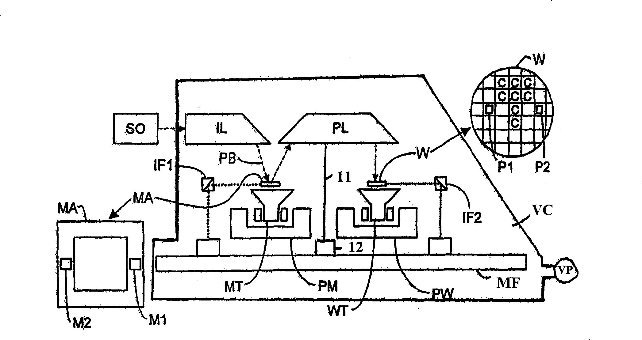
[0039] figure 1 A lithographic apparatus according to a particular embodiment of the invention is schematically shown. The unit includes:

[0040] - an illumination system (illuminator) IL for providing a projection beam PB of radiation, such as UV radiation or EUV radiation;

[0041] - a first support structure (eg mask table) MT for supporting the patterning device (eg mask) MA, connected to first positioning means PM for precise positioning of the patterning device relative to the object PL;

[0042] - a substrate table (e.g. a wafer table) WT for holding a substrate (e.g. a resist-coated wafer) W connected to a second positioning device PW for precise positioning of the substrate relative to the object PL; and

[0043] - A projection system (eg reflective projection lens) PL for imaging the pattern applied to the projection beam PB by the patterning device MA on a target portion C of the substrate W (eg comprising one or more dies).

[0044] As described herein, the de...


PUM


Abstract

A lithographic apparatus comprising projection optics (PL) for projecting a patterned light beam onto a target portion of a substrate. The projection optics assembly comprises a first element (4) having a predetermined function, which is fixedly positioned relative to a second element (2), wherein the elements (4, 2) are arranged in spaced relation on a support frame (6), supporting The frame (6) is provided with an interface interface (8) formed on or in the frame (6) for accommodating the first component (4), and the interface interface (8) determines that the first component (4) is relatively The position of the two elements (2) is adjustable according to the predetermined function, so that the first element (4) can be positioned relative to the second element (2) in at least three degrees of freedom.

Description

technical field [0001] The invention relates to an assembly comprising a first element having a predetermined function, wherein the first element can be fixedly positioned relative to a second element. For example, the present invention also relates to a lithographic apparatus and device manufacturing method, but is not limited in this respect. Background technique [0002] A lithographic apparatus is a machine that can apply a desired pattern on a target portion of a substrate. A lithographic apparatus may be used, for example, in the manufacture of integrated circuits (ICs). In this case, a patterning device such as a mask can be used to create a circuit pattern corresponding to the individual layers of the IC that can be imaged onto a substrate (such as a silicon wafer) with a layer of radiation-sensitive material (anti- etchant) on a target portion (eg, including one or more dies). Typically, a single substrate contains a network of adjacent target portions that are s...

Claims


Application Information

Patent Timeline
Patent Type & Authority Patents(China)
IPC IPC(8): G03F7/20H01L21/00H01L21/027
CPCG03F7/70825G03F7/20
Inventor D·J·P·A·弗兰肯
Owner ASML NETHERLANDS BV
Why Eureka
Try Eureka