Making method for NAND-type quick flash memory selective bar

A manufacturing method and selection gate technology, applied in semiconductor/solid-state device manufacturing, semiconductor devices, electrical components, etc., can solve the problem of photoresist residue or peeling, incomplete transfer of selection gate patterns, inability to manufacture non-type flash memory, etc. problem, to achieve the effect of increasing the area

Active Publication Date: 2009-03-11
SEMICON MFG INT (SHANGHAI) CORP +1
View PDF8 Cites 0 Cited by
  • Summary
  • Abstract
  • Description
  • Claims
  • Application Information

AI Technical Summary

Problems solved by technology

[0016] The problem to be solved by the present invention is to provide a method for fabricating a selection gate of a NAND flash memory, so as to prevent photoresist residue or peeling due to exposure energy lower than or higher than the actual required exposure energy of the photoresist, resulting in poor pattern transfer of the selection gate. Integrity, defects are generated in the subsequent process of making the selection gate, and it is impossible to make a complete NAND flash memory

Method used


Image

  • Making method for NAND-type quick flash memory selective bar
  • Making method for NAND-type quick flash memory selective bar
  • Making method for NAND-type quick flash memory selective bar

Examples


Embodiment Construction

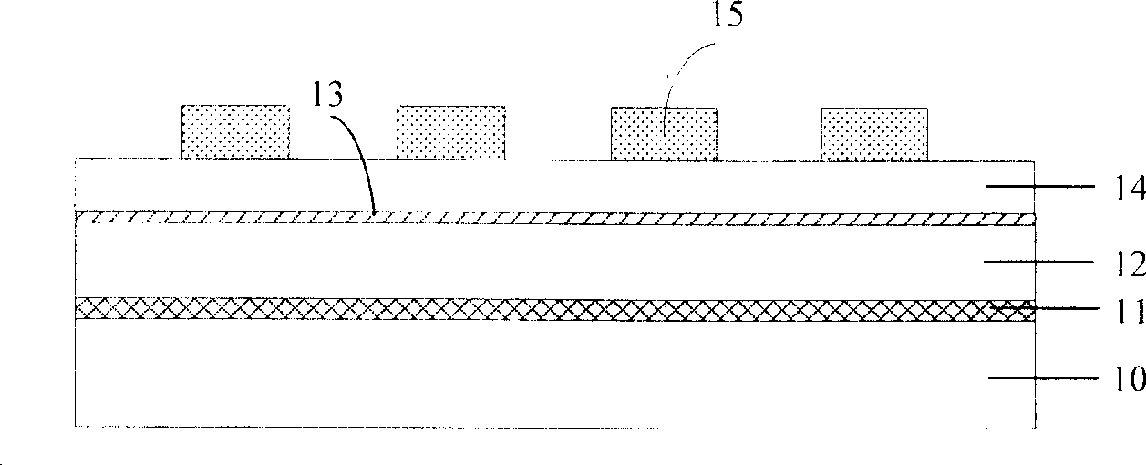
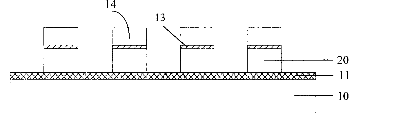
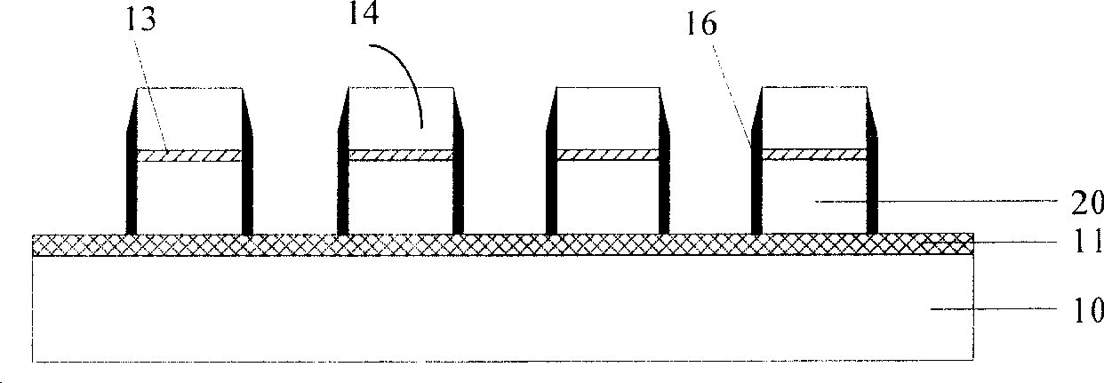
[0027] Because in the existing manufacturing process of non-type flash memory, when defining the position of the selection gate on the photoresist, the photoresist is deposited into the trench between each semiconductor device, because the critical dimension of the semiconductor device is getting smaller and smaller, Then the trenches between the semiconductors will be smaller, and it is difficult for the light to irradiate completely vertically during photolithography, and it is easy to generate diffuse reflection on the surface of the photoresist. The invention directly coats a layer of photoresist on the flat surface of the polysilicon conductive layer instead of depositing photoresist in the grooves between semiconductor devices. In this way, the exposed area increases, the light will not change the transmission direction because the illuminated area is too small, and there will be no diffuse reflection on the surface of the photoresist, so there will be no exposure energy ...


PUM


Abstract

A method for manufacturing selecting grid of nand flash memory comprises the following steps: a polysilicon conducting layer is deposited on a wafer; the polysilicon conducting layer is polished; the surface of the polysilicon conducting layer is covered with optical resistances; the graph on the optical cover is transferred onto the optical resistance to define the selecting grid; the optical resistance, which limits the position of the selecting grid, remains after developing, while the rest optical resistances are removed; the polysilicon conducting layers of the removed optical resistances are corroded; the optical resistance at the position of the selecting grid is removed; the polysilicon conducting layer on the wafer is corroded as a whole; the selecting grid is formed. The corroding process is carried out after the optical resistance on the surface of the polysilicon conducting layer defines the selecting grid, thus completely solving the problem of the residual and peeling of the optical resistances during the process of exposure.

Description

technical field [0001] The invention relates to a semiconductor storage device, in particular to a manufacturing method of a selection gate of a NAND flash memory. Background technique [0002] Flash memory is a type of non-volatile memory that can retain on-chip information even after the power supply is turned off; it is electrically erasable and reprogrammable in the system without requiring a special high voltage; flash memory has low cost, The characteristic of high density. Its unique performance makes it widely used in various fields, including embedded systems, such as PCs and peripherals, telecommunication switches, cellular phones, network interconnection equipment, instrumentation and automotive devices, as well as emerging voice, image, data Storage products such as digital cameras, digital voice recorders and personal digital assistants. [0003] NAND technology is a kind of flash memory, which has the following characteristics: (1) read and program operations...

Claims


Application Information

Patent Timeline
Patent Type & Authority Patents(China)
IPC IPC(8): H01L21/768H01L21/8247H01L21/28
Inventor 刘蓓洪中山隋建国金贤在
Owner SEMICON MFG INT (SHANGHAI) CORP
Why Eureka
Try Eureka