
Data processing circuit with multiplexed memory

A memory circuit and data processing technology, applied in electrical digital data processing, instrumentation, climate sustainability, etc., can solve the problems of limited operation speed and high power consumption of equipment

Inactive Publication Date: 2009-04-29
卡莱汉系乐有限公司
View PDF4 Cites 0 Cited by
  • Summary
  • Abstract
  • Description
  • Claims
  • Application Information

AI Technical Summary

Problems solved by technology

[0004] The disadvantage of high memory speed is that it consumes a lot of power and limits the speed at which the device can operate

Method used

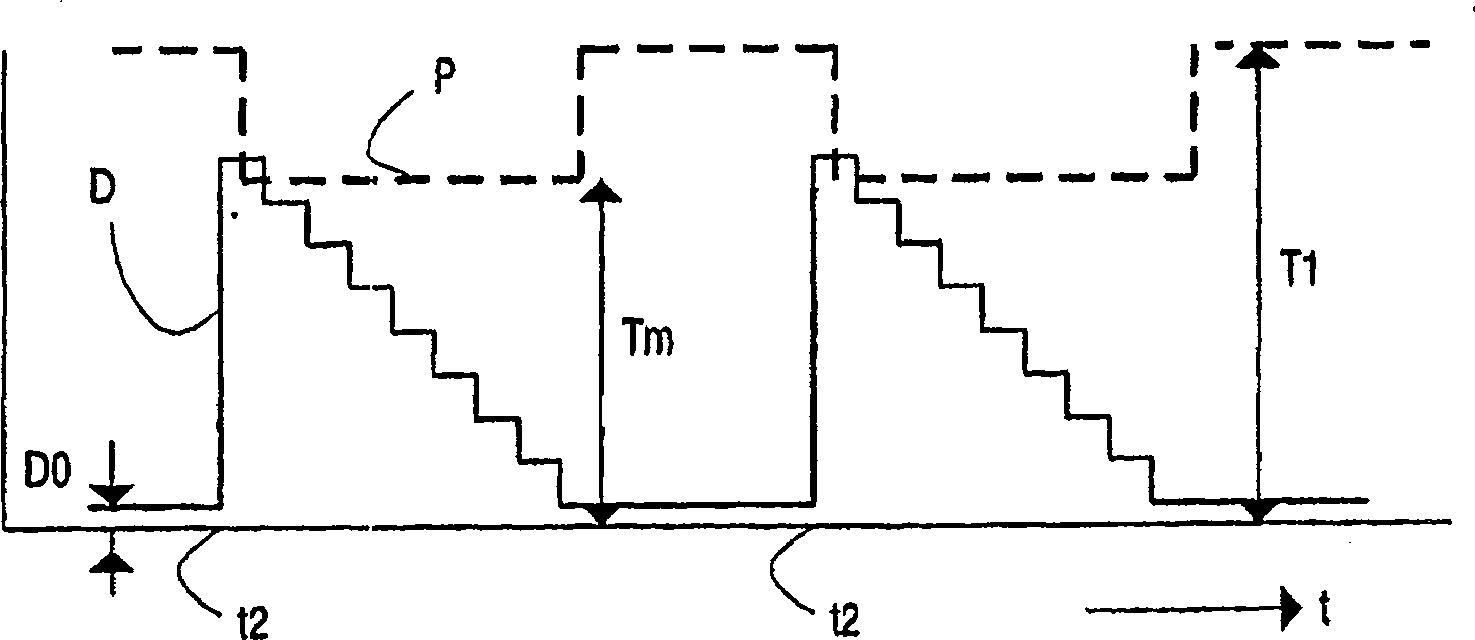
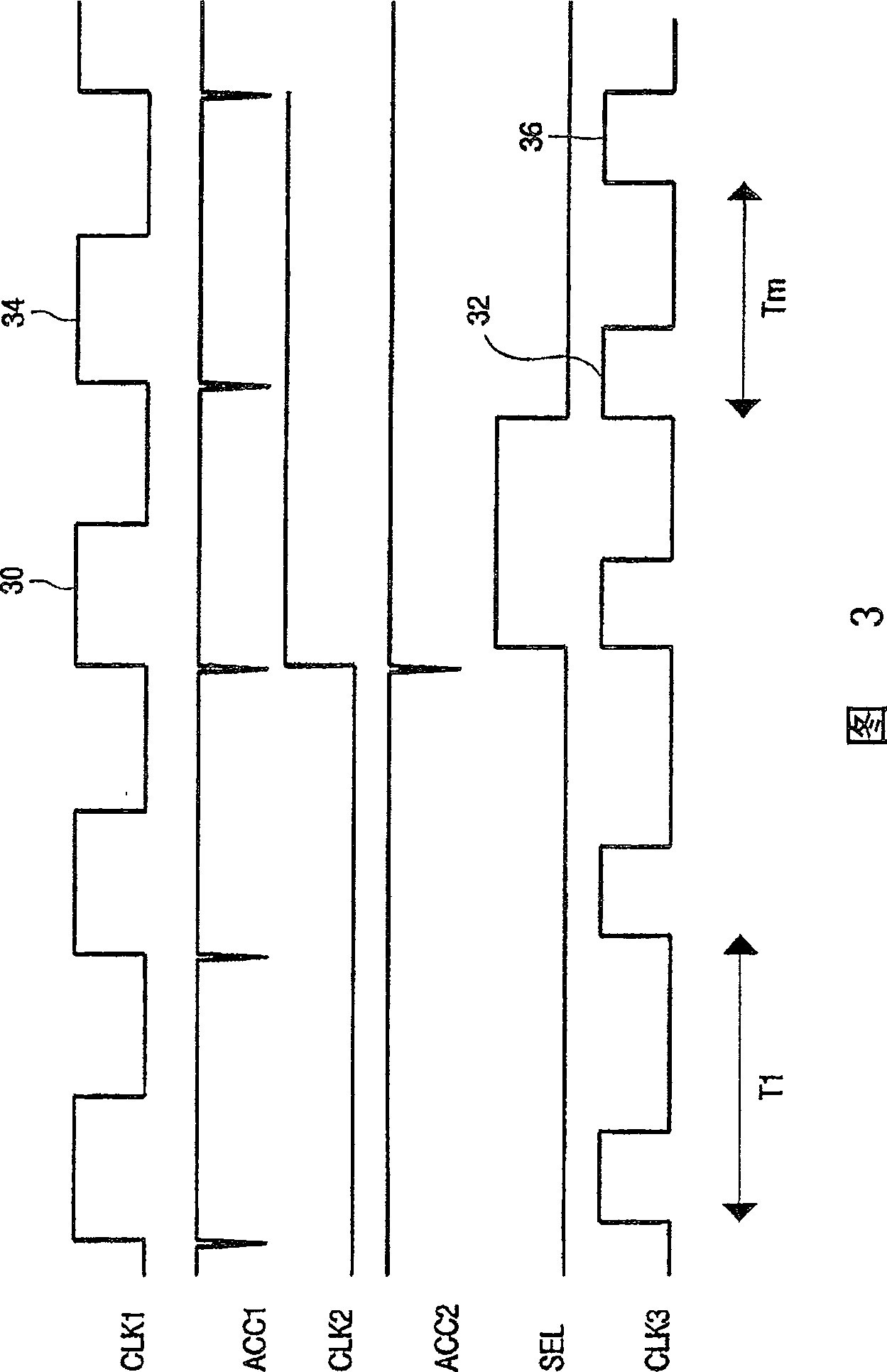

Image

  • Data processing circuit with multiplexed memory
  • Data processing circuit with multiplexed memory
  • Data processing circuit with multiplexed memory

Examples


Embodiment Construction

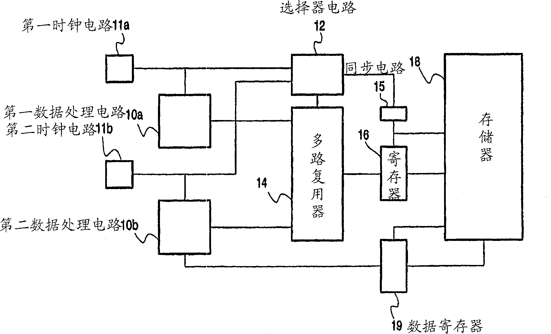
[0030] figure 1 A circuit is shown with a first data processing circuit 10a, a second data processing circuit 10b, a first clock circuit 11a, a second clock circuit 11b, a selector circuit 12, a multiplexer 14, a synchronization circuit 15 , register 16, memory 18 and data register 19. The first clock circuit 11 a is coupled to the first data processing circuit 10 a and the selector circuit 12 . The second clock circuit 11 b is coupled to the second data processing circuit 10 b and the selector circuit 12 . The first and second data processing circuits 10a, b have an access request information output coupled to an input of a multiplexer 14 which in turn has an output coupled to an input of a register 16 . Selector circuit 12 has a select output coupled to the control input of multiplexer 14 and a timing control output coupled to synchronization circuit 15 . Synchronization circuit 15 has a timing output coupled to register 16 and memory 18 . The data register 19 has an inp...


PUM


Abstract

A data processing apparatus contains several processing circuits each operating under control of its own periodic clock signal, so that the clock signals may have different frequencies and / or can be autonomous. The several processing circuits each have an output for outputting memory access requests, which remain at the output for a validity duration interval defined by the clock signal of the particular processor. A multiplexing circuit multiplexes the access requests to a memory. The memory needs a minimum memory repetition period before it can accept an access request following acceptance of a preceding access request. The clock periods of the processing circuits are longer than the minimum memory repetition period. A timing circuit selects acceptance time points at which each particular access request from a first data processing circuit is accepted.

Description

technical field [0001] The invention relates to a device in which processing performed by different circuits accesses the same single-port memory circuit. Background technique [0002] In theory, multi-port memory could be an ideal technology for enabling different circuits to independently access the same memory circuit. But in practice, actual multi-port memories are not popular because they contain a lot of system overhead compared with traditional single-port memories. Therefore, single-port memories are often used to implement pseudo-multiport memories. [0003] From US Patent 5,706,482, published January 6, 1998, a device is known with a pseudo multi-port memory comprising a single-port memory for storing image data. Both the first circuit performing write processing and the second circuit performing read processing can access the memory. A FIFO write queue is provided between the memory port and the first circuit, and a FIFO read queue is provided between the memor...

Claims


Application Information

Patent Timeline
IPC IPC(8): G06F13/16
CPCG06F13/1673G06F13/1642Y02D10/00G06F13/16G06F13/00
Inventor J·L·W·克斯塞斯I·安德烈杰
Owner 卡莱汉系乐有限公司
Learn More