Positive temperature coefficient polycrystalline silicon resistor structure and manufacturing method thereof

A polysilicon resistance, positive temperature coefficient technology, applied in resistors, circuits, electrical components, etc., can solve the problems of inability to obtain polysilicon resistance structure design, limitations, etc., to avoid performance limitations and excellent process stability.

Active Publication Date: 2019-04-26
SHANGHAI HUAHONG GRACE SEMICON MFG CORP
View PDF6 Cites 0 Cited by
  • Summary
  • Abstract
  • Description
  • Claims
  • Application Information

AI Technical Summary

Problems solved by technology

In order to obtain a positive temperature coefficient resistance structure with a higher resistance value, it is generally obtained through the process of the above-mentioned diffusion region resistance or well region resistance. The disadvantage is that the accuracy or area is sacrificed. When the resistance accuracy requirements are very strict, the design is limited by the inability to obtain a polysilicon resistance structure with a positive temperature coefficient

Method used


Image

  • Positive temperature coefficient polycrystalline silicon resistor structure and manufacturing method thereof
  • Positive temperature coefficient polycrystalline silicon resistor structure and manufacturing method thereof
  • Positive temperature coefficient polycrystalline silicon resistor structure and manufacturing method thereof

Examples


Embodiment Construction

[0033] The present invention is described in detail below in conjunction with accompanying drawing:

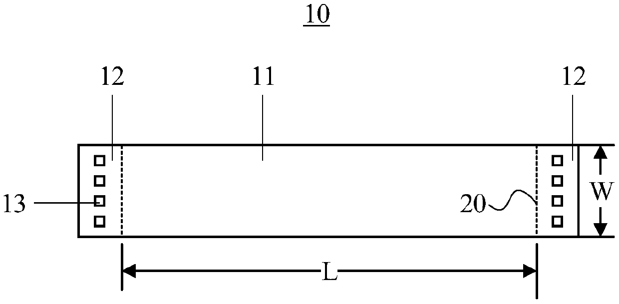
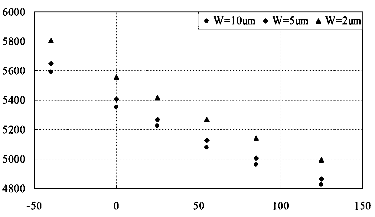
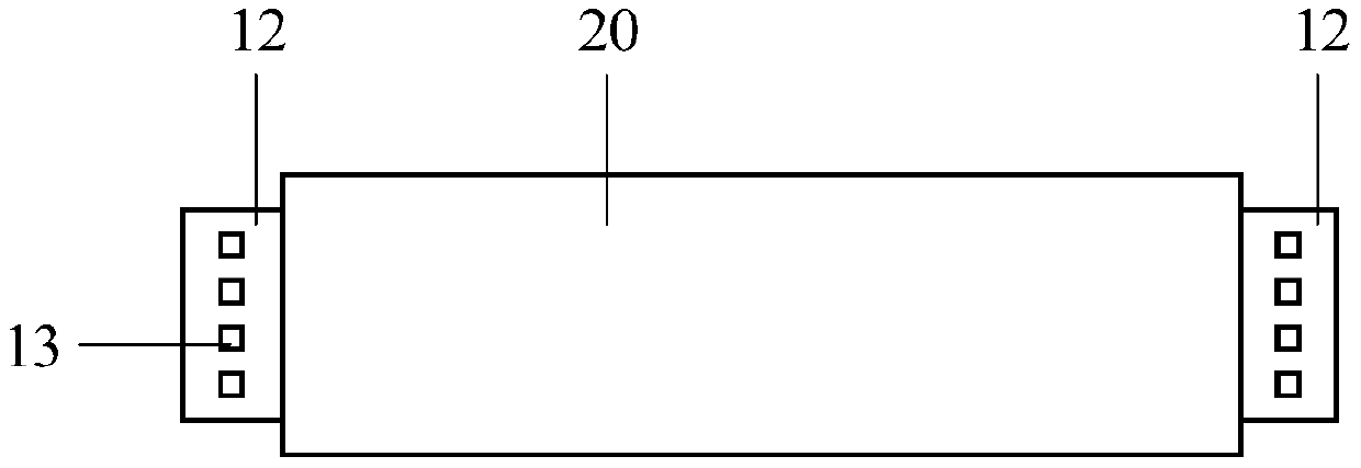
[0034] image 3 It is a structural schematic diagram of a metal silicide barrier layer covering the middle area of ​​a traditional non-metallized polysilicon resistor. Please refer to image 3 , due to the polysilicon resistance structure in the manufacturing process, by setting the metal silicide barrier layer 20 in the middle region 11 to prevent the metallization of the middle region 11, and the exposed end region 12 is generally provided with a contact hole 13 through the metal silicide metal connected by metal wires. Figure 4 is a curve diagram of the resistance value of the middle region of the polysilicon resistance structure changing with temperature; Figure 5 It is a graph showing the variation of resistance value with temperature after the end region of the polysilicon resistance structure is metallized with metal silicide. Wherein the abscissa is the temperatu...


PUM

PropertyMeasurementUnit
widthaaaaaaaaaa

Abstract

The invention provides a positive temperature coefficient polycrystalline silicon resistor structure and a manufacturing method thereof. The positive temperature coefficient polycrystalline silicon resistor structure comprises a plurality of polycrystalline silicon unit resistors which each comprise a nonmetallic polycrystalline silicon region and metallic polycrystalline silicon regions, whereineach nonmetallic polycrystalline silicon region is located in a middle region, a resistance value of each nonmetallic polycrystalline silicon region changes with a negative temperature coefficient, the metallic polycrystalline silicon regions are located at end regions, and resistance values of the metallic polycrystalline silicon regions change with a positive temperature coefficient. The adjacent polycrystalline silicon unit resistors are connected with metal wires with resistance values changing with a positive temperature coefficient through contact holes formed in the end regions. According to the manufacturing method, the ratio of the nonmetallic polycrystalline silicon regions relative to the metallic polycrystalline silicon regions is adjusted, and thus the positive changing amountof the resistance values of the metallic polycrystalline silicon regions along with temperatures is greater than or equal to the negative changing amount of the resistance values of the nonmetallic polycrystalline silicon regions along with temperatures. The positive temperature coefficient polycrystalline silicon resistor structure can avoid limitation of the performance of semiconductor devices, and high resistance values can be obtained under the conditions that process burden is not increased, device process stability is guaranteed and the area is not sacrificed.

Description

technical field [0001] The invention relates to the technical field of semiconductor manufacturing, in particular to a positive temperature coefficient polysilicon resistance structure and a manufacturing method thereof. Background technique [0002] Semiconductor resistance devices are one of the most widely used devices in semiconductor chip products, and the temperature characteristics of resistance are very important in product applications. Commonly used resistors are as follows. The resistance formed by using polysilicon material on the semiconductor substrate through the isolation of the oxide layer is called polysilicon (Poly) resistance. Please refer to Figure 14 , the relationship between the resistance of the diffusion region and the position of the polysilicon resistance is as follows. Taking the P-type silicon substrate as an example, it includes a P-type silicon substrate 301, an N-type diffused region resistor 302, an oxide layer 303, and a polysilicon resi...

Claims


Application Information

Patent Timeline
Patent Type & Authority Applications(China)
IPC IPC(8): H01L23/64
CPCH01L23/647H01L28/20
Inventor 张昊辛海维
Owner SHANGHAI HUAHONG GRACE SEMICON MFG CORP
Why Eureka
Try Eureka