On-chip system

A system-on-chip and device technology, applied in the field of system-on-chip, can solve problems such as internal bus communication bottlenecks, reduce system performance, and prolong system running time, so as to avoid compromise processing, increase communication bandwidth, and facilitate design reuse.

Active Publication Date: 2009-05-06
SUGON INFORMATION IND
View PDF3 Cites 0 Cited by
  • Summary
  • Abstract
  • Description
  • Claims
  • Application Information

AI Technical Summary

Problems solved by technology

The bandwidth of the data bus is the maximum communication bandwidth of the entire system. If the control\status information and other data are transmitted using the same data bus, the various functional modules in the system need to exchange data frequently. When the maximum communication bandwidth required by the entire system exceeds the bandwidth of the data bus, the internal bus becomes the communication bottleneck
Especially when multiple functional modules compete for the same bus resource, the central arbitrator will only allow one functional module to use the resource at a time, and other functional modules must wait, and some functional modules need to wait for a long time to obtain the right to use the bus , the insertion of a large number of waiting cycles will prolong the running time of the system and greatly reduce the performance of the system

Method used


Image

  • On-chip system
  • On-chip system
  • On-chip system

Examples


Embodiment Construction

[0035] The present invention will be further described in detail below in conjunction with the accompanying drawings and specific embodiments.

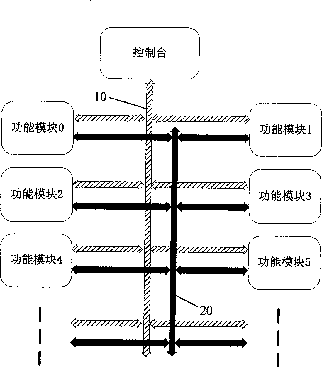
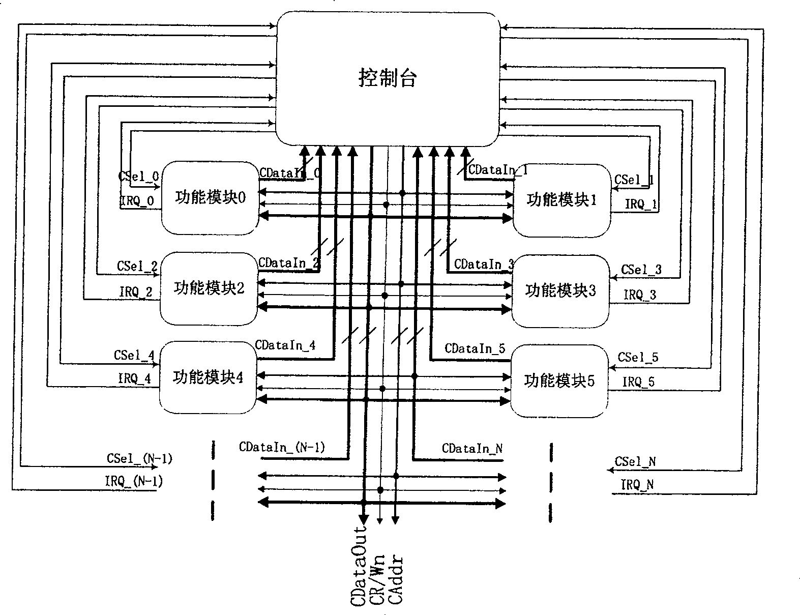
[0036] A system-on-chip usually includes a plurality of functional modules, and each functional module has a bus interface, and is connected by an internal bus of the system-on-chip. In the present invention such as figure 1 In the illustrated embodiment, the system-on-chip includes functional modules 0-5 (expandable) and a console. The console is a special functional module of the system-on-chip, and is often served by an embedded RISC CPU or a functional module with the same or similar functions as the RISC CPU. In other possible embodiments, the console can also be integrated into other functional modules. As will be apparent from the description below, the console will act as the master device in the control / status channel of the present invention.

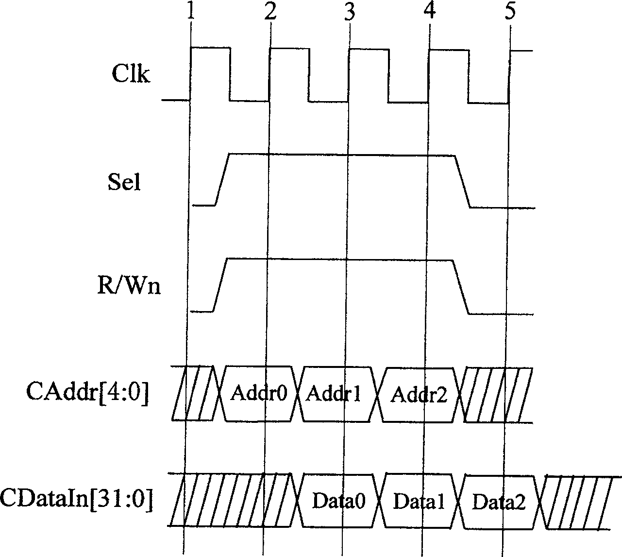
[0037] Such as figure 1 As shown, in the present invention, the internal bus ...


PUM


Abstract

The on-chip system includes several functional modules connected with internal bus including two independent transmission channels, including one control / state channel for transmitting control / state information and one data channel for transmitting other data except control / state information. Each of the control / state channel and the data channel has separate data bus, address bus and control bus. The kernel of the present invention is to design on-chip system bus in the strategy of separate control / state channel and data channel, which have different topologic structures and communication protocols. The present invention has greatly simplified interface design of functional modules inside the system and increased total system communication bandwidth, and is especially suitable for on-chip system design with compact data interaction.

Description

technical field [0001] The present invention relates to the field of semiconductor chips, and more specifically, relates to a system on chip. Background technique [0002] With the development of semiconductor technology level to deep submicron and the further improvement of EDA tools, more and more complex functional modules (usually IP modules) can be integrated inside the chip to form a complex system-on-a-chip (System-on-a- chip, SoC). In general, a large amount of data needs to be exchanged between various functional modules, and these data exchanges are completed by communication links, so the communication link often becomes the bottleneck of system performance. According to whether the functional modules share the communication link, the communication link can be divided into a point-to-point mode and a bus mode. If each functional module within the system is connected by a shared communication link, the system architecture is based on the bus. Each functional mod...

Claims


Application Information

Patent Timeline
Patent Type & Authority Patents(China)
IPC IPC(8): G06F13/38
Inventor 刘新春张佩珩江先阳李晓民孙凝晖
Owner SUGON INFORMATION IND
Why Eureka
Try Eureka