Transport method and transport apparatus for semiconductor wafer
A technology of transportation device and transportation method, which is applied in the direction of transportation and packaging, semiconductor/solid-state device manufacturing, and printing equipment, etc., which can solve the problems of reduced output and defects, and achieve the effect of avoiding the reduction of output
- Summary
- Abstract
- Description
- Claims
- Application Information
AI Technical Summary
Problems solved by technology
Method used
Image

Examples
no. 1 example
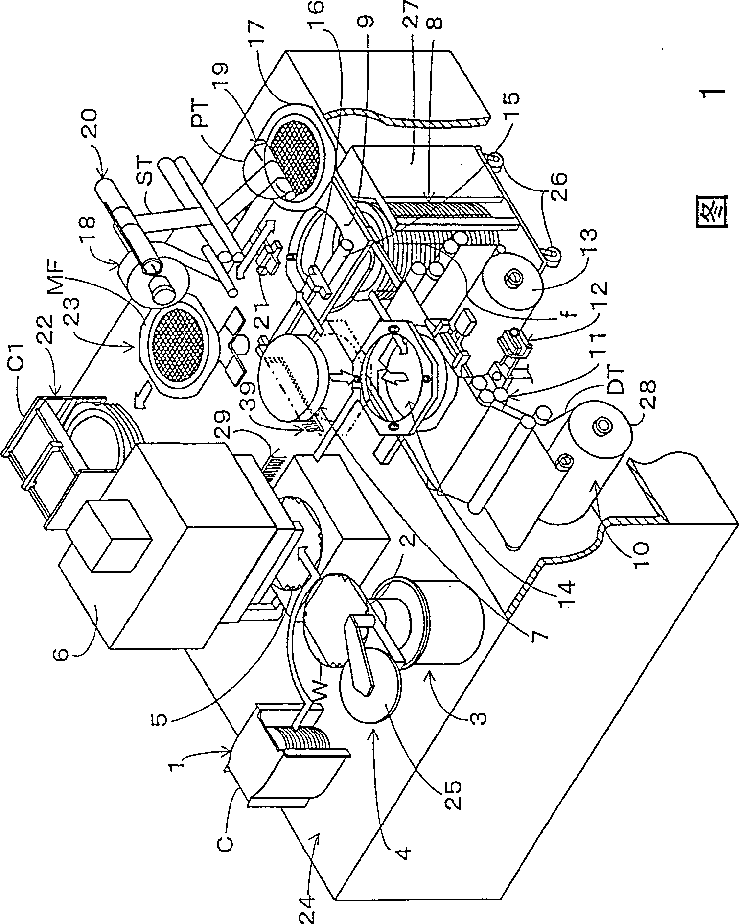
[0054] 1 is a partially cutaway perspective view of the entire structure of an embodiment of a semiconductor wafer mounting apparatus equipped with a semiconductor wafer transport apparatus according to the present invention. Note that in this embodiment, an ultraviolet curing adhesive tape as a surface protection tape is attached to the pattern surface (front surface) of the semiconductor wafer W (hereinafter also simply referred to as "wafer W").
[0055] A semiconductor wafer mounting apparatus includes: a wafer supply station 1, wherein a cassette C accommodating a wafer W is loaded, the mask (back mask) of the back surface on the wafer has been completed, and the wafers are stacked into multiple layers; a wafer transport mechanism 3, which has a robot arm 2 that pivots while being bent; a wafer pressing mechanism 4 used to straighten a warped wafer W; an alignment table 5 used as a wafer holding device, on which The upper wafer W is placed-held and aligned; an ultraviolet...
no. 2 example
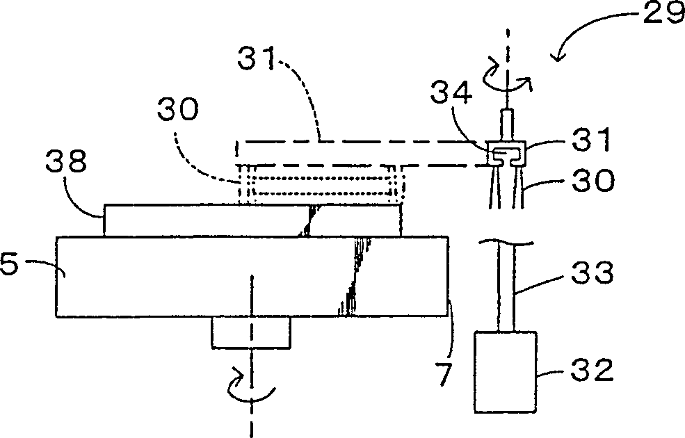
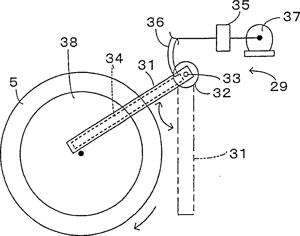
[0107] In the second embodiment, a structure is adopted in which a first wafer cleaning mechanism 290 is provided instead of the alignment table cleaning mechanism 29 as the dust removal device of the first embodiment.
[0108] Therefore, components having the same structure as those of the first embodiment are attached with the same reference numerals, and detailed descriptions are given only for components having structures different therefrom.
[0109] FIG. 7 is a partially cutaway perspective view of an entire structure of an embodiment of a semiconductor wafer mounting apparatus equipped with a semiconductor wafer transport apparatus according to the present invention.
[0110] Such as wafer cleaning mechanism 290 ( Figure 8 ) side view and top plan view of the main part ( Figure 9 ), the first wafer cleaning mechanism 290 as a dust removal device is arranged near the alignment table 5.
[0111] The first wafer cleaning mechanism 290 is structured as follows: the firs...
PUM
 Abstract
Description
Claims
Application Information
 - R&D
- Intellectual Property
- Life Sciences
- Materials
- Tech Scout
- Unparalleled Data Quality
- Higher Quality Content
- 60% Fewer Hallucinations
Browse by: Latest US Patents, China's latest patents, Technical Efficacy Thesaurus, Application Domain, Technology Topic, Popular Technical Reports.
© 2025 PatSnap. All rights reserved.Legal|Privacy policy|Modern Slavery Act Transparency Statement|Sitemap|About US| Contact US: help@patsnap.com