Photoetching equipment and device manufacturing method
A kind of equipment and lithography projection technology, applied in the direction of micro-lithography exposure equipment, semiconductor/solid-state device manufacturing, electrical components, etc., can solve the problems of reflectivity reduction, optical system light reduction, etc.
- Summary
- Abstract
- Description
- Claims
- Application Information
AI Technical Summary
Problems solved by technology
Method used
Image
Examples
Embodiment 1
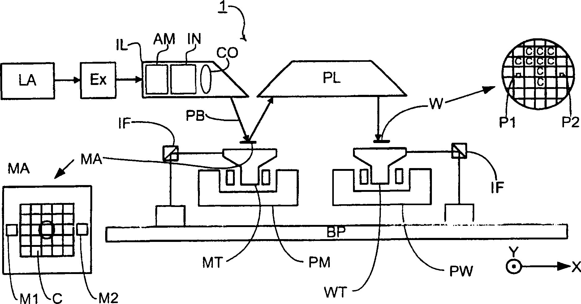
[0048] figure 1 A lithographic projection apparatus according to a specific embodiment of the present invention is schematically shown. The unit includes:
[0049] a radiation system Ex, IL for providing a projection beam PB of radiation (e.g. EUV radiation), which in this particular case also includes a radiation source LA;
[0050] A first target stage (mask stage) MT configured with a mask holder for holding a mask MA (e.g. a reticle) and with a first positioner for precisely positioning the mask relative to the element PL device connection;
[0051] A second target stage (substrate stage) WT configured with a substrate holder for holding a substrate W (e.g., a silicon wafer coated with a protective layer) and connected to a second target stage for precise positioning of the substrate relative to the element PL Two positioning devices are connected.
[0052] A projection system ("lens") PL (eg mirror set) for imaging the radiation portion of mask MA onto a target portio...
Embodiment 2
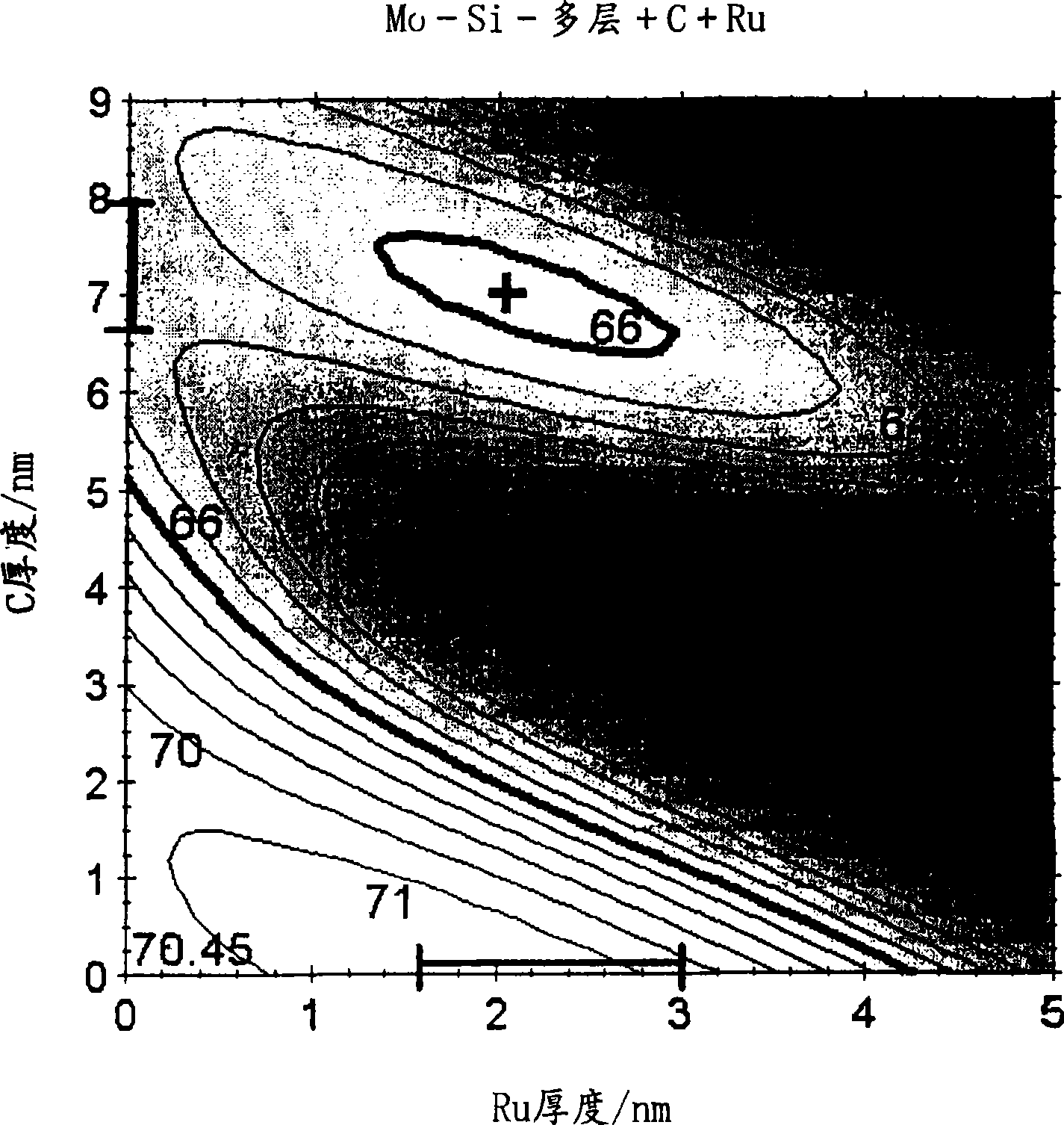
[0066] image 3 The results of simulated calculation of the theoretical reflectance of the normal incidence optical element according to the second embodiment are shown. The optical element of this second embodiment has the same structure as that of the first embodiment except that the interlayer is composed of C instead of Mo.
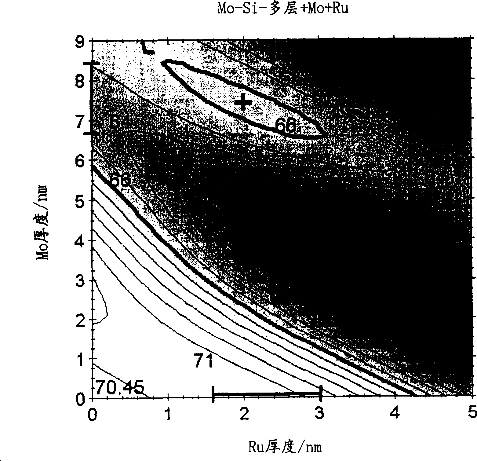
[0067]As in the first embodiment, from image 3 It is evident that the second peak of reflectivity occurs when the interlayer thickness is between 6.0 nm and 9.0 nm. The highest reflectance is seen between 6.5 nm and 8.2 nm, especially between 7.0 nm and 7.8 nm. For the Ru capping layer, the optimum reflectivity occurs between 1.6nm and 3.0nm. For a greater thickness of the interlayer, a smaller thickness of the capping layer is desired, for example as little as 1.0 nm. For smaller thickness interlayers composed of C, it is desirable to have a larger Ru capping layer thickness up to about 3.0 nm. Preferably the Ru capping layer has a thickness be...
Embodiment 3
[0069] Figure 4 The results of simulated calculation of the theoretical reflectance of the normal incidence optical element according to the third embodiment of the present invention are shown. The structure of the optical element of the third embodiment of the invention is the same as that of the first embodiment of the invention, except that the interlayer consists of an inner layer of Mo positioned next to the multilayer structure and an outer layer of C positioned next to the Ru cladding layer. Figure 4 The simulation results in correspond to a Mo interlayer thickness of 3.36 nm.
[0070] Figure 4 The results in the figure 2 and 3 The results for the second peak of reflectance are displayed in the same manner as the results for the second peak of reflectance. For a capping layer composed of Ru having a thickness above about 2.0 nm, more preferably above 2.2 nm, and most preferably above about 2.4 nm, the second peak of the reflectance in the third embodiment occurs...
PUM
| Property | Measurement | Unit |
|---|---|---|
| thickness | aaaaa | aaaaa |
| thickness | aaaaa | aaaaa |
| thickness | aaaaa | aaaaa |
Abstract
Description
Claims
Application Information


