
Lithographic apparatus and device manufacturing method

a technology of lithographic projection and manufacturing method, which is applied in the direction of magnetic recording, record information storage, vacuum evaporation coating, etc., can solve the problems of significant decrease in reflectivity, and achieve the effect of improving resistance to oxidation and acceptable reflectivity

Inactive Publication Date: 2005-10-11
ASML NETHERLANDS BV +1
View PDF8 Cites 1 Cited by
  • Summary
  • Abstract
  • Description
  • Claims
  • Application Information

AI Technical Summary

Benefits of technology

The present invention provides an optical element that has good reflectivity and is resistant to oxidation over the long term. This is achieved by using a special structure called a Si / Mo multilayer, which includes an interlayer between the multilayer and the capping layer. The interlayer has a thickness of between 6.0 and 9.0 nm or includes an inner interlayer of Mo next to the multilayer and an outer interlayer of C, with the outer interlayer having a thickness greater than 3.4 nm or the capping layer has a thickness greater than 2.0 nm. This interlayer ensures that the capping layer material does not intermix with the outer layer of the multilayer structure. The optical element can be used in a lithographic apparatus to project a patterned beam of radiation onto a target portion of a layer of radiation-sensitive material at least partially covering a substrate. The invention has many applications, such as in the manufacture of ICs, integrated optical systems, guidance and detection patterns for magnetic domain memories, liquid-crystal display panels, thin-film magnetic heads, etc.

Problems solved by technology

Surprisingly, this increase in oxidation resistance is not accompanied by a significant decrease in reflectivity, which would be disadvantageous.

Method used


Image

  • Lithographic apparatus and device manufacturing method
  • Lithographic apparatus and device manufacturing method
  • Lithographic apparatus and device manufacturing method

Examples


first embodiment

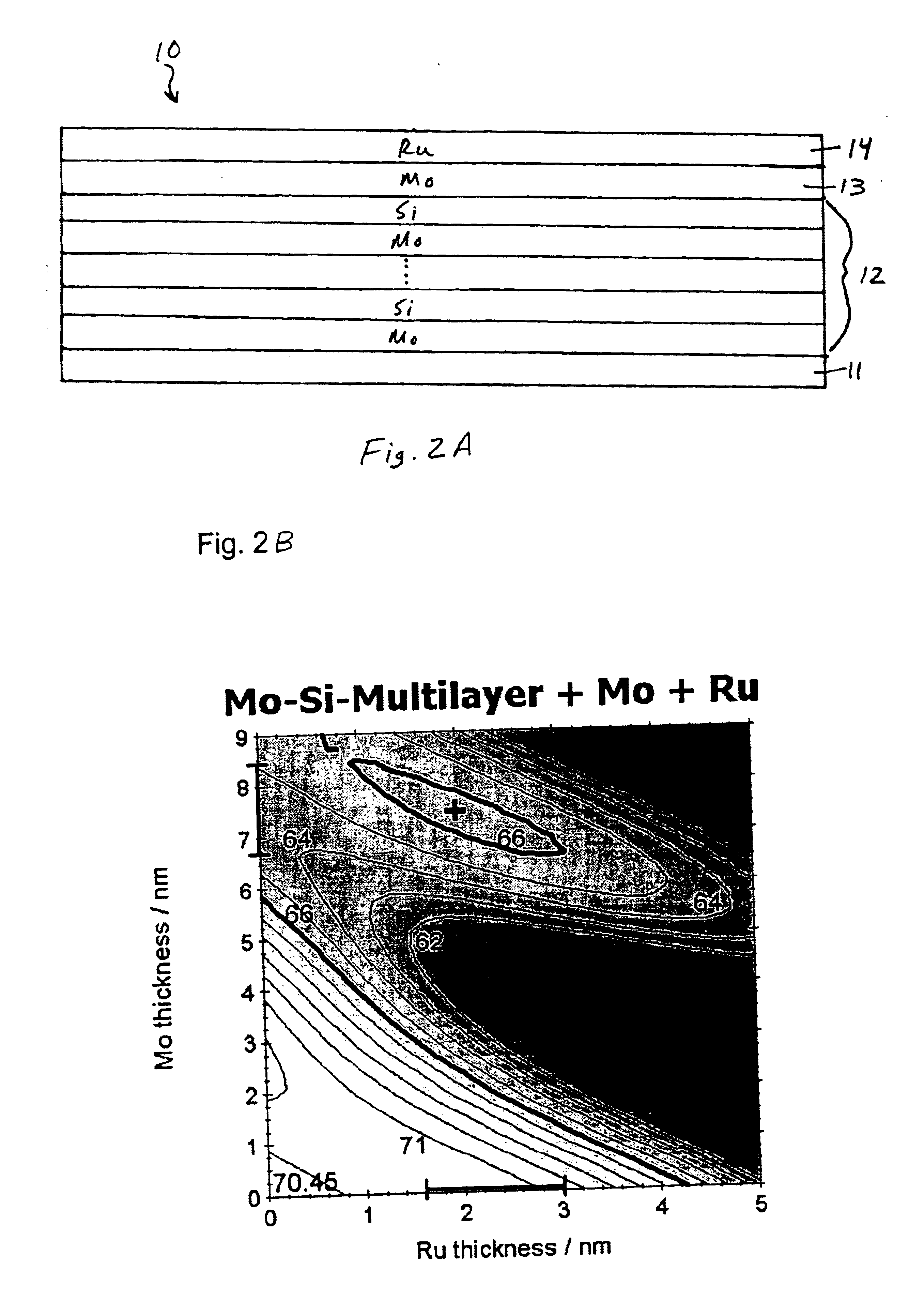
[0044]As with the first embodiment, a second peak in reflectivity is apparent from FIG. 3B in the case where the interlayer 13A has a thickness of between 6.0 and 9.0 nm. The highest reflectivity is seen between 6.5 and 8.2 nm and more particularly between 7.0 and 7.8 nm. For the capping layer of Ru, the best reflectivity is between 1.6 and 3.0 nm.

[0045]For a larger thickness of the interlayer, a lower thickness of the capping layer is desirable, for example as low as 1.0 nm. For a lower thickness of the interlayer 13A of C a larger thickness of Ru capping layer 14 is desirable, up to about 3.0 nm. Preferably the Ru capping layer 14 has a thickness of between 1.6 and 3.0 nm, more preferably at least 2.0 nm.

[0046]Referring to FIGS. 4A and 4B, FIG. 4B shows the results of simulations calculating the theoretical reflectivity of a normal incidence optical element 10B according to the third embodiment of the present invention. The structure of the optical element 10B of the third embodim...

third embodiment

[0047]The results in FIG. 4B show a second peak of reflectivity in the same way that the results in FIGS. 2B and 3B also show a second peak in reflectivity. The second peak in reflectivity in the third embodiment occurs with an outer interlayer of C with a thickness of between 3.0 to 4.0 nm, for a capping layer of Ru with a thickness greater than about 2.0 nm, more preferably 2.2, and most preferably greater than about 2.4 nm. For a capping layer of Ru with a thickness of between 1.6 and 3.0, the best reflectivity is achieved with an outer interlayer of C of at least 3.4 nm, preferably greater than about 3.5 nm and most preferably greater than about 3.7 nm.

[0048]As can be seen from the examples, the second peak in reflectivity occurs when the interlayer thickness, i.e. the thickness of those layers positioned between the outermost Si layer in the Si / Mo multilayer structure and the capping layer, is about half the wavelength of the incident radiation, between 0.3 and 0.7, or between ...


PUM

PropertyMeasurementUnit
thicknessaaaaaaaaaa
thicknessaaaaaaaaaa
thicknessaaaaaaaaaa

Abstract

An optical element of a lithographic projection apparatus includes a Si / Mo multilayer structure, an outer capping layer and an interlayer positioned between the multilayer structure and the outer capping layer. The interlayer has a thickness of between 0.3 and 0.7 times the wavelength of the incident radiation. The interlayer may be C or Mo and has a thickness of between 6.0 and 9.0 nm. The interlayer may include an inner interlayer including Mo next to the multilayer structure and an outer interlayer including C next to the capping layer. The outer interlayer is at least 3.4 nm thick and the capping layer is Ru and at least 2.0 nm thick.

Description

RELATED APPLICATION[0001]This application claims the benefit of priority to European Patent Application No. 02255961.1, filed Aug. 28, 2002, the contents of which are herein incorported by reference.BACKGROUND OF THE INVENTION[0002]1. Field of the Invention[0003]The present invention relates to a lithographic projection apparatus and a device manufacturing method.[0004]2. Description of the Related Art[0005]The term “patterning device” as here employed should be broadly interpreted as referring to device that can be used to endow an incoming radiation beam with a patterned cross-section, corresponding to a pattern that is to be created in a target portion of the substrate. The term “light valve” can also be used in this context. Generally, the pattern will correspond to a particular functional layer in a device being created in the target portion, such as an integrated circuit or other device (see below). An example of such a patterning device is a mask. The concept of a mask is wel...

Claims


Application Information

Patent Timeline
Patent Type & Authority Patents(United States)
IPC IPC(8): G21K1/00G21K1/06G03F7/20G21K5/00G21K5/02H01L21/027
CPCB82Y10/00G21K1/062Y10T428/24355Y10T428/30G03F7/20
Inventor KURT, RALPHYAKSHIN, ANDREI EVGENUEVICH IAKCHINE
Owner ASML NETHERLANDS BV
Learn More