Display device

A technology of display device and display screen, which can be used in identification devices, lighting devices, instruments, etc., and can solve problems such as area reduction.

Inactive Publication Date: 2009-07-22
SOLAS OLED LTD
View PDF3 Cites 0 Cited by
  • Summary
  • Abstract
  • Description
  • Claims
  • Application Information

AI Technical Summary

Problems solved by technology

[0004] However, when optical components such as microlens arrays and prism sheets are placed on the display surface of the flat panel display, the output rate of light to the front is improved, but there are problems as follows: For example, if the red pixel (R) that emits light Among the radially radiated light, the light that reaches above the green pixel (G) adjacent to the red pixel (R) is refracted or reflected by the optical component facing the green pixel (G) and is emitted in the front direction, and the light from the red pixel (G) is emitted to the front. The light emitted by the pixel (R) is superimposed on the original light-emitting pixel of the green pixel (G), and only the area of ​​the color of the green pixel (G) is reduced

Method used


Image

  • Display device
  • Display device
  • Display device

Examples


Deformed example 1

[0096] Below, use Figure 5A , Figure 5B Modification 1 will be described.

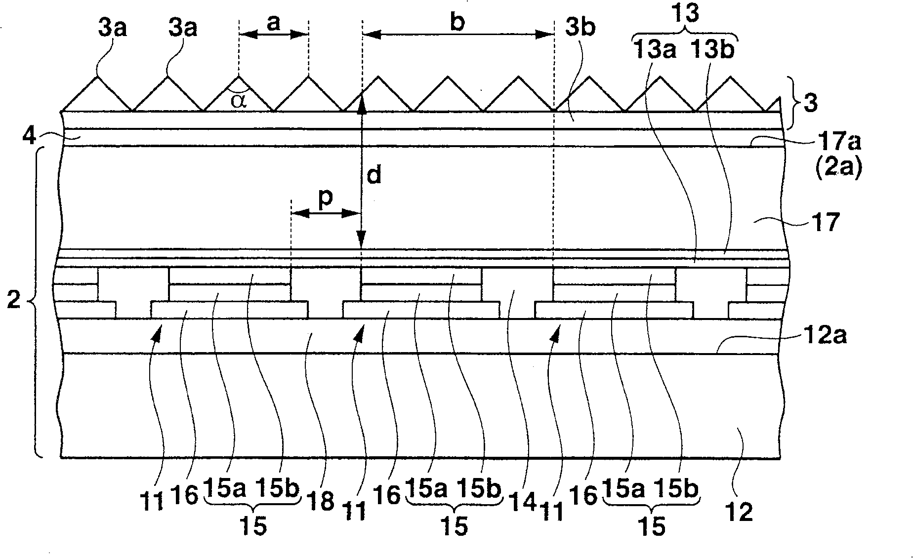
[0097] In the display device of Modification 1, the sealing film 17 is partitioned by the spacer 5 . That is, on the common electrode 13 , the spacer 5 having a mesh shape in plan view is formed corresponding to the insulating film 14 . By forming the separators 5 in a mesh shape in a plan view, a plurality of cells surrounded by the separators 5 are arranged in a matrix. In addition, the EL layer 15 is arranged in each cell when viewed from above. The sealing film 17 is filled in each cell formed by the separator 5 . The film thickness of the spacer 5 is the same as that of the sealing film 17 , and the optical sheet 3 is adhered to the flat surface 2 a formed by the sealing film 17 and the spacer 5 via the optical adhesive 4 . The spacer has better light-shielding performance and the best reflective performance to the light emitted by the EL layer 15 . The display device of Modification 1 has...

Deformed example 2

[0100] Hereinafter, modification 2 will be described with reference to FIGS. 6A and 6B .

[0101] In the display device of embodiment 1, the optical sheet 3 is bonded on the surface 2a of the flat panel display 2; and in the display device of modification example 2, as shown in Fig. 6A and Fig. 6B, many microprisms 3a are passed through light The engraving is formed directly on the surface 2a of the flat panel display 2. Here, there is an interval between adjacent microprisms 3a, which is the same as the width of the non-light-emitting area between laterally adjacent pixels. In addition, one microprism 3a is arranged opposite to a longitudinal column of pixels. In addition to the above, the display device of Modification 2 is the same as Figure 5A , Figure 5B The display device of Modification 1 shown has the same structure.

Deformed example 3

[0103] Below, use Figure 7A , FIG. 8A to describe Modification 3.

[0104] In the display device of Modification 1, there is no space between adjacent microprisms 3a of the optical sheet 3, and one slope of the microprism 3a intersects the other slope of the adjacent microprism 3a. On the other hand, in the display device of Modification 3, if Figure 7A , Figure 7B Shown, there is interval between the adjacent microprisms 3a of optical sheet 3, between adjacent microprisms 3a, form the bottom surface 3b that is roughly parallel with the back side of optical sheet 3, an inclined plane of microprism 3a intersects with bottom surface 3b, Another slope of the adjacent microprism 3a crosses the bottom surface 3b. In addition, one microprism 3 a is arranged opposite to the longitudinal row of pixels, and the bottom surface 3 b is opposite to the spacer 5 . In addition to the above, the display device of Modification 3 is the same as Figure 5A , Figure 5B The display devic...


PUM

PropertyMeasurementUnit
thicknessaaaaaaaaaa
refractive indexaaaaaaaaaa
heightaaaaaaaaaa

Abstract

A display device comprises a flat display panel and an optical sheet. The flat display panel has a surface on which a plurality of pixels are arranged into a matrix. The pixels are coated with a light permeable material. The optical sheet provides a front directivity of the flat display panel. Light which is emitted from a predetermined pixel of the plural pixels and emitted in an outside front direction from a surface of the optical sheet disposed on a region other than the relevant pixel, has a width overlapping the neighboring pixel arranged around the relevant pixel. The width is 20% or lower than the pixel width of the neighboring pixel.

Description

technical field [0001] The invention relates to a display device using a flat panel display such as an electroluminescent (EL) display. Background technique [0002] In recent years, research and development of flat panel displays has been actively carried out. Among flat-panel displays, there are liquid crystal displays using transmitted light, plasma displays using discharge phenomena, field emission displays, and EL displays using electroluminescence phenomena. In the case of displaying by a dot matrix method, pixels are arranged in a matrix no matter what kind of display screen. [0003] In order to improve the visibility of a flat panel display, optical processing may be applied to the display surface of the flat panel display. For example, in order to suppress the reflection of external light on the display surface of the flat panel display, an AR (Anti Reflection, anti-reflection) coating may be coated on the display surface of the flat panel display. In addition, ...

Claims


Application Information

Patent Timeline
Patent Type & Authority Patents(China)
IPC IPC(8): G09F9/30H05B33/22G02B5/04G02F1/1335H01J5/16H01J61/40H01L51/52H05B33/00
CPCH01J2329/897H01J2211/442H01L51/5268G02F1/133524H01L51/5284H01L51/5281G02F2001/133562G02B5/045H01J2211/44G02F1/133562H10K50/854H10K50/86H10K50/865H05B33/22
Inventor 武居学白崎友之
Owner SOLAS OLED LTD
Why Eureka
Try Eureka