PMOS tube production method capable of improving instability of negative temperature

A technology of instability and manufacturing method, applied in semiconductor/solid-state device manufacturing, electrical components, circuits, etc., can solve the problems of large Vt drift, PMOS negative temperature instability, Idsat increase, etc., to reduce the threshold voltage Drift, the effect of alleviating the effect of negative temperature instability, reducing the effect of saturation leakage current

Inactive Publication Date: 2010-01-27
SEMICON MFG INT (SHANGHAI) CORP +1
View PDF5 Cites 0 Cited by
  • Summary
  • Abstract
  • Description
  • Claims
  • Application Information

AI Technical Summary

Problems solved by technology

[0004] However, because the above-mentioned reaction temperature is too high and the nitrogen content is too high, the content of hydrogen contained in the silicon nitride made is low, that is, the hydrogen-silicon bonds formed are less, and hydrogen is easy to diffuse at the interface, so a large amount of nitrogen gas is produced. Interface state, so that the negative temperature instability of the fabricated PMOS is obvious, that is, its Vt drifts greatly and Idsat increases significantly after pressurization or high temperature

Method used


Image

  • PMOS tube production method capable of improving instability of negative temperature

Examples


Embodiment Construction

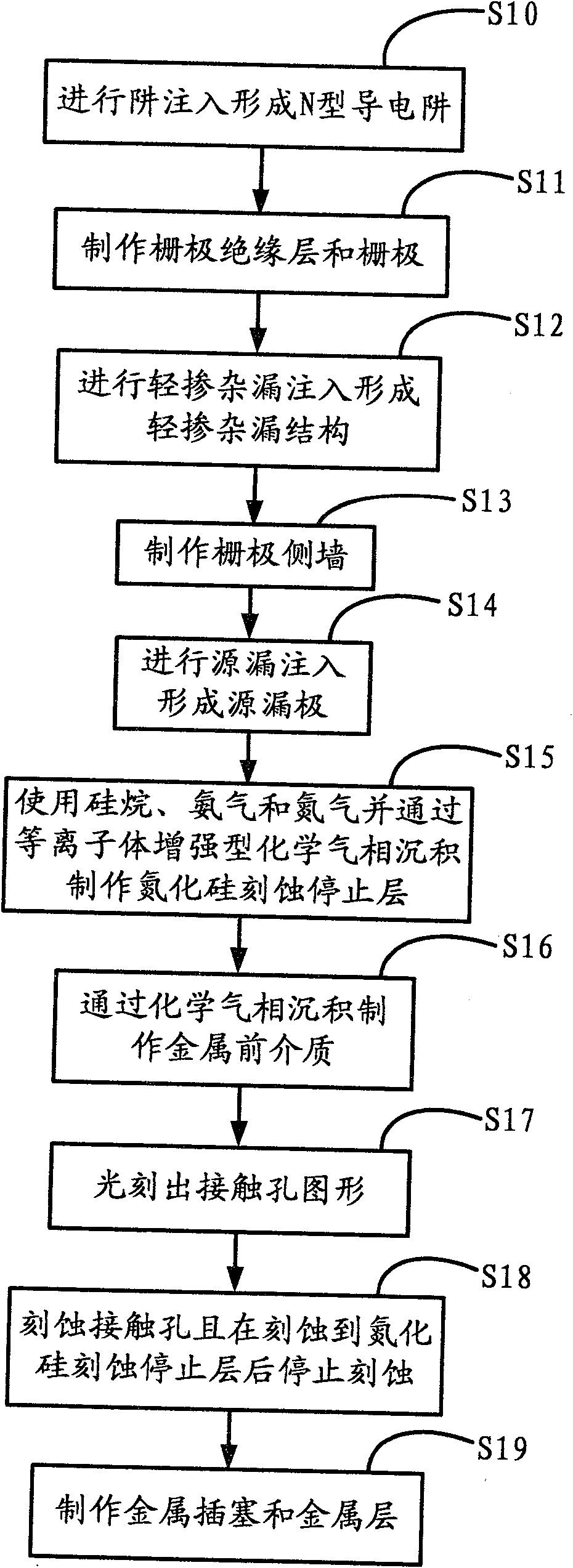
[0013] The following will further describe in detail the manufacturing method of the PMOS transistor capable of improving the negative temperature instability of the present invention.

[0014] see figure 1 According to the PMOS transistor manufacturing method capable of improving the negative temperature instability of the present invention, the first step S10 is to perform well implantation to form an N-type conductive well. In this embodiment, an N-type conductive well is formed by phosphorus doping.

[0015] Then continue to step S11 , forming a gate insulating layer and a gate, wherein the gate insulating layer is silicon oxynitride or silicon oxide, and the gate is a polysilicon gate.

[0016] Then continue to step S12, perform lightly doped drain implantation to form a lightly doped drain structure. In this embodiment, the lightly doped impurity is boron fluoride.

[0017] Then continue to step S13 , making gate sidewalls.

[0018] Then continue to step S14, perform...


PUM


Abstract

The invention provides a method for preparing a PMOS pipe which can improve the negative-temperature instability. In the prior art, when a silicon nitride etching and stopping layer is prepared, hydrogen-silicon keys which are formed in silicon nitride by adopting nitrogen with higher temperature and larger flow are less, thus, the hydrogen on an interface is easy to diffuse, and consequently, the PMOS pipe has the phenomenon by the influence of NBT1 that the Vt excursion is larger, and Idsat is larger. The method for preparing the PMOS pipe comprises the following steps: the trap injection is firstly carried out; next, a grid insulating layer, a grid and a lightly doped drain structure are prepared; then, the side wall of the grid and a source-drain electrode are prepared; and next, the silicon nitride etching and stopping layer is prepared, wherein the flow range of the nitrogen is from 0 to 10 standard state milliliters / minute, the aggradation temperature range is from 390 to 410 DEG C, then, metal front media is prepared, and a contact hole is prepared according to the silicon nitride etching and stopping layer; and finally, a metal plug and a metal layer are prepared. The negative-temperature instability of the PMOS pipe can be obviously improved by the method of the invention, and the Vt excursion and the Idsat of the PMOS pipe are correspondingly reduced.

Description

technical field [0001] The invention relates to a PMOS tube manufacturing process, in particular to a PMOS tube manufacturing method capable of improving negative temperature instability. Background technique [0002] For P-channel Metal Oxide Semiconductor Field Effect Transistor (PMOS), negative temperature instability (Negative Bias Temperature Instability, referred to as NBTI) is the main cause of its degradation under pressure or high temperature. The NBTI effect is generally considered to be caused by the hydrogen-silicon bond breakage at the interface and the diffusion of hydrogen, resulting in parameter drift and device degradation (such as threshold voltage (Vt) drift and saturation leakage current (Idsat) increase), so it needs to be controlled by Process related to hydrogen to improve NBTI effect. [0003] In the process of making PMOS, after completing the making of the gate, source and drain, before making the metal layer, a silicon nitride layer will be made o...

Claims


Application Information

Patent Timeline
Patent Type & Authority Patents(China)
IPC IPC(8): H01L21/336
Inventor 甘正浩吴永坚郑凯廖金昌
Owner SEMICON MFG INT (SHANGHAI) CORP
Why Eureka
Try Eureka