Method for forming copper layer and copper mosaic structure

A technology of copper inlaid structure and copper layer, which is applied in the direction of electrical components, semiconductor/solid-state device manufacturing, circuits, etc., can solve the problems of pores in copper layer or copper inlaid structure, improve the quality of formation, reduce the quantity, and simple operation Effect

Inactive Publication Date: 2010-02-17
SEMICON MFG INT (SHANGHAI) CORP +1
View PDF4 Cites 0 Cited by
  • Summary
  • Abstract
  • Description
  • Claims
  • Application Information

AI Technical Summary

Problems solved by technology

[0011] The invention provides a method for forming a copper layer and a copper inlaid structure, so as to improve the problem that pores easily appear in the copper layer or the copper inlaid structure in the existing forming method

Method used


Image

  • Method for forming copper layer and copper mosaic structure
  • Method for forming copper layer and copper mosaic structure
  • Method for forming copper layer and copper mosaic structure

Examples


Embodiment Construction

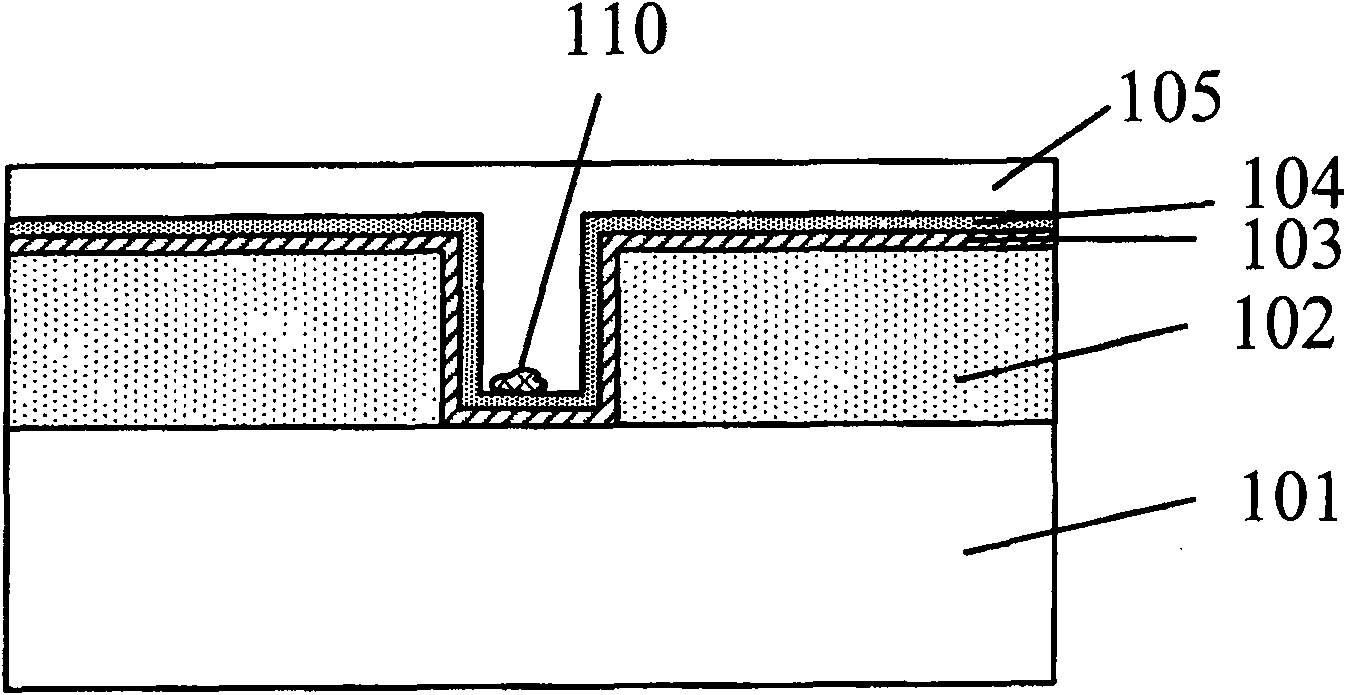
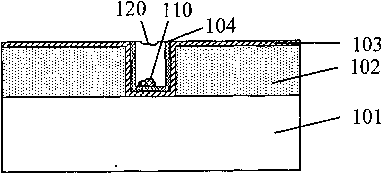
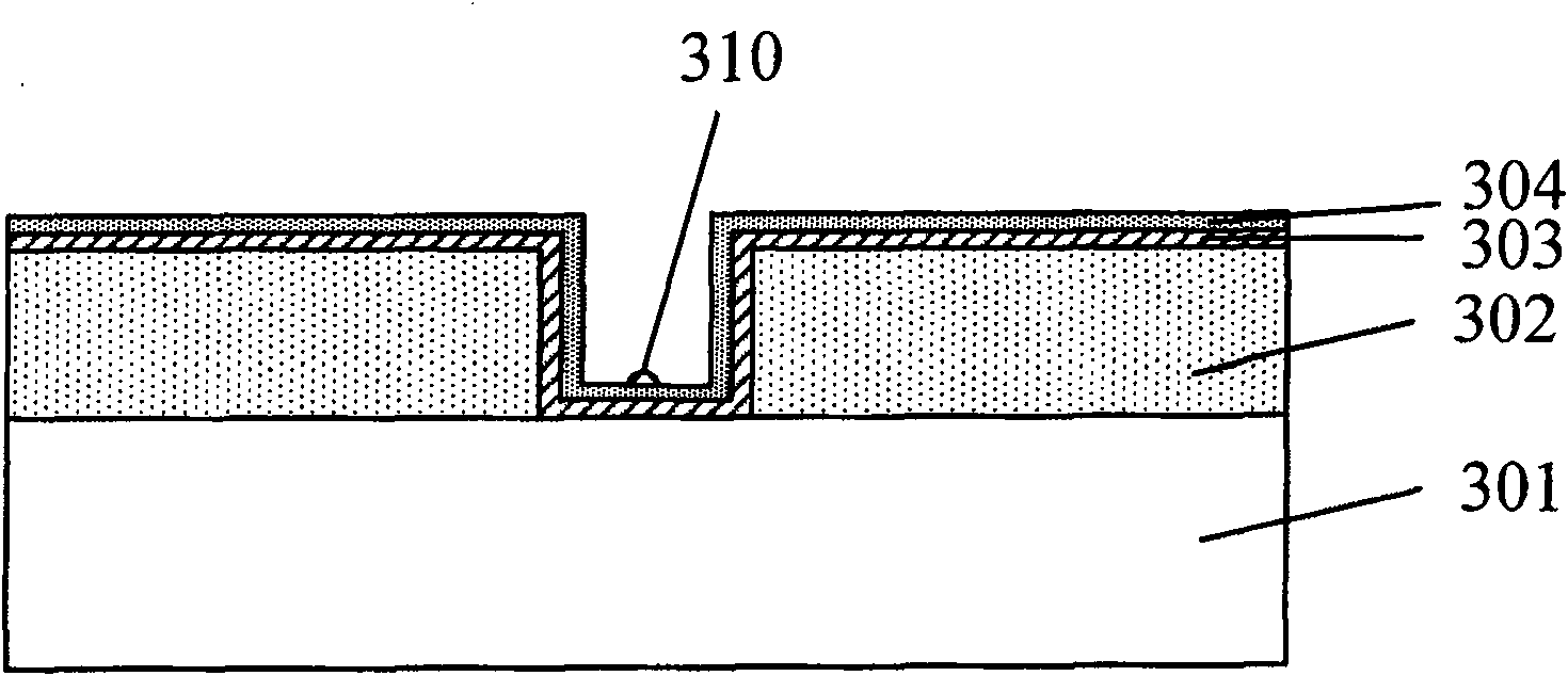
[0057] In order to make the above objects, features and advantages of the present invention more comprehensible, specific implementations of the present invention will be described in detail below in conjunction with the accompanying drawings.

[0058] The processing method of the present invention can be widely used in various fields, and can utilize many suitable materials to make, and the following is to illustrate by specific embodiment, certainly the present invention is not limited to this specific embodiment, in this field Common replacements known to those of ordinary skill undoubtedly fall within the protection scope of the present invention.

[0059] Secondly, the present invention is described in detail using schematic diagrams. When describing the embodiments of the present invention in detail, for the convenience of explanation, the cross-sectional view showing the device structure will not be partially enlarged according to the general scale, which should not be u...


PUM


Abstract

The invention discloses a copper layer formation method, including the following steps: providing a substrate which is provided with a copper inoculating crystal layer on the surface; transferring thesubstrate into copper electroplating equipment; introducing protecting gas into the annealing device of the copper electroplating equipment and processing a first annealing treatment to the substrate; electroplating copper on the substrate through the electroplating device of the electroplating equipment; processing fringe washing treatment to the substrate through the fringe washing device of the electroplating equipment; and processing a second annealing treatment to the substrate through the annealing device of the copper electroplating equipment. In this way, the process of electroplatingthe copper can be finished. The invention further discloses a corresponding copper mosaic structure formation method. The copper mosaic structure formation method can effectively reduce the number ofthe pores in the copper layer, thus improving the quality of the copper layer or the copper mosaic structure.

Description

technical field [0001] The invention relates to the technical field of semiconductor manufacturing, in particular to a method for forming a copper layer and a copper inlaid structure. Background technique [0002] As the production of integrated circuits develops towards ultra-large-scale integrated circuits (ULSI), the internal circuit density is increasing, and the number of components contained is increasing, so that the surface of the wafer cannot provide enough area to make the required interconnection lines. (Interconnect). In order to meet the increased demand for interconnection lines after the shrinkage of components, the design of multilayer metal interconnection lines with more than two layers realized by using through holes has become a method that must be adopted in VLSI technology. [0003] The traditional metal interconnection is made of aluminum metal, but with the continuous shrinking of the device feature size in the integrated circuit chip, the current de...

Claims


Application Information

Patent Timeline
Patent Type & Authority Patents(China)
IPC IPC(8): H01L21/3205H01L21/768
Inventor 王文琦聂佳相康芸杨瑞鹏
Owner SEMICON MFG INT (SHANGHAI) CORP
Why Eureka
Try Eureka