Check patentability & draft patents in minutes with Patsnap Eureka AI!

Semiconductor encapsulation structure and its making method

A packaging structure, semiconductor technology, applied in the direction of semiconductor/solid-state device manufacturing, semiconductor devices, semiconductor/solid-state device components, etc., can solve the problems of occupying printed circuit boards, unable to configure passive components, large connection area, etc., to achieve enhanced Electrical function, the effect of improving electrical function and quality

Inactive Publication Date: 2007-08-01
SILICONWARE PRECISION IND CO LTD
View PDF6 Cites 1 Cited by
  • Summary
  • Abstract
  • Description
  • Claims
  • Application Information

AI Technical Summary

Problems solved by technology

[0005] The common problem with the above packaging structure is that the pins used to electrically connect to external devices such as printed circuit boards protrude out of the encapsulant, so they often occupy a large area of ​​the printed circuit board.
This packaging structure cannot be used to package semiconductor chips with center pads, cross-shaped or I-shaped arrays, such as DRAM chips.
[0012] In addition, passive components cannot be configured in the above-mentioned various packaging structures to improve the electrical function of the packaging structure

Method used


Image

  • Semiconductor encapsulation structure and its making method
  • Semiconductor encapsulation structure and its making method
  • Semiconductor encapsulation structure and its making method

Examples


Embodiment 1

[0040] Please refer to FIG. 5A to FIG. 5E , which are schematic cross-sectional views of Embodiment 1 of the semiconductor package structure and its manufacturing method of the present invention.

[0041] Embodiment 1 of the present invention is mainly described in a batch manner, so as to improve the process efficiency and enable mass production. Of course, it can also be performed in a single wafer manner, and is not limited thereto.

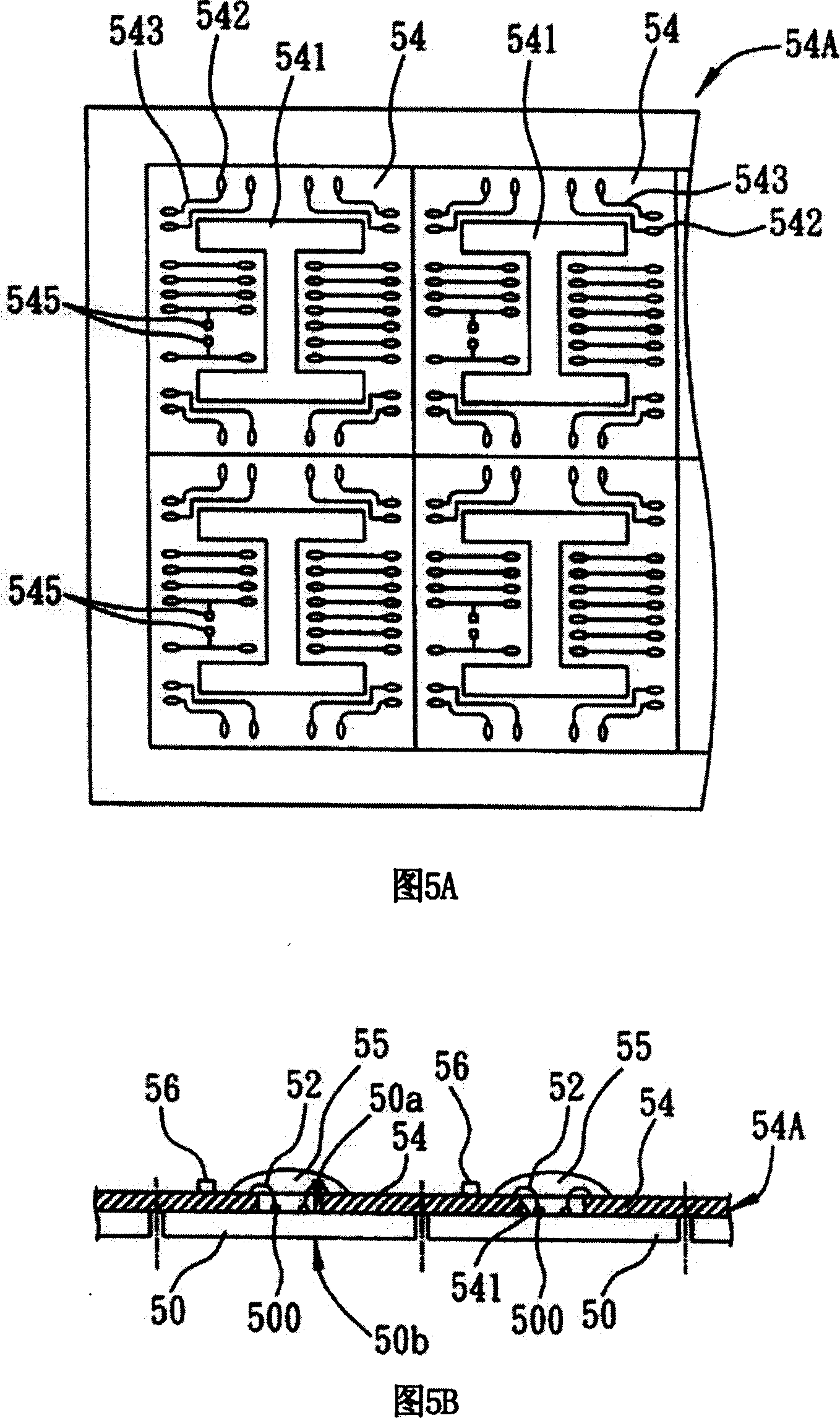
[0042] The manufacturing method of the semiconductor package structure of the present invention includes the following steps. As shown in FIG. 5A, it provides a substrate module sheet 54A with a plurality of substrates 54, and each of the substrates 54 is formed with at least one opening 541, and the form of the opening 541 is corresponding to the semiconductor chip to be packaged subsequently. The layout arrangement of the pads on the active surface. In this embodiment, the bonding pads on the active surface of the semiconductor chip to be p...

Embodiment 2

[0050] Please also refer to FIG. 6A to FIG. 6D , which are schematic cross-sectional views of Embodiment 2 of the semiconductor package structure and its manufacturing method of the present invention.

[0051] The manufacturing method of the semiconductor package of the present invention includes: as shown in FIG. 6A , providing a lead frame 51 with a plurality of pins 511, and each of the pins 511 has an inner edge 511a and an outer edge 511b that form a gap. The height of the outer edge 511b of the pin is greater than the height of the inner edge 511a, and the semiconductor chip 50 is placed on the inner edge 511a of the pin. The semiconductor chip 50 has an active surface 50a and an opposite non-active surface 50b, and the semiconductor chip 50 is connected to the inner edge 511a of the pin with its non-active surface 50b, and the active surface 50a of the semiconductor chip is provided with a welding pad 500 .

[0052] As shown in Figure 6B, a substrate 54 is placed on th...

Embodiment 3

[0057] Please also refer to FIG. 7 , which is a schematic cross-sectional view of Embodiment 3 of the semiconductor package structure of the present invention.

[0058] Embodiment 3 of the present invention is substantially the same as Embodiment 1 above, the main difference is that the size of the substrate 54 is larger than the size of the semiconductor chip 50, for the semiconductor chip 50 to be placed on the inner edge 511a of the pin 511, and to be connected to the semiconductor chip. The substrate 54 on the lead frame 50 is electrically connected to the pin inner edge 511 a of the lead frame 51 .


PUM


Abstract

The invention discloses a semiconductor encapsulation structure and its production method, the structure includes: semiconductor chip, base plate, weld wire, lead rack equipped with many feet and encapsulation colloid. The semiconductor encapsulation structure and its production method in the invention can be used in encapsulate various of semiconductor chips equipped with different types of weld cushion array, so encapsulation structure which without outer feet and possesses light-minded and short property, at the same time, the stack can be encapsulated and the passive components can be connected to increase the power function.

Description

technical field [0001] The invention relates to a semiconductor packaging structure and its manufacturing method, in particular to a semiconductor packaging structure with an integrated lead frame and its manufacturing method. Background technique [0002] The traditional thin small outline package (Thin Small Outline Package, TSOP) is mainly to connect the semiconductor chip on a lead frame with multiple pins on both sides, and then use the encapsulant to cover the semiconductor chip, so as to use two The extended part of the side pin is electrically connected with the outside. [0003] As shown in Figure 1, it is the sectional schematic diagram of traditional TSOP, and it comprises a lead frame 11, and this lead frame 11 has a chip holder 111 and a plurality of pins 112 that are located at this chip holder 111 both sides; The semiconductor chip 10 on the chip holder 111, and the semiconductor chip 10 is electrically connected to the pin 112 by the bonding wire 12; 13 , a...

Claims


Application Information

Patent Timeline
IPC IPC(8): H01L23/488H01L23/31H01L21/60H01L21/56
CPCH01L2924/01015H01L2924/01082H01L2224/4824H01L2224/4826H01L2224/97H01L2224/32245H01L2224/48247H01L2224/73215H01L24/97H01L2924/01005H01L2924/01033H01L2924/18165H01L2924/01006H01L2224/48455H01L2224/48091H01L2924/181H01L2924/00014H01L2224/85H01L2924/00012
Inventor 黄建屏张锦煌
Owner SILICONWARE PRECISION IND CO LTD
Features
  • R&D
  • Intellectual Property
  • Life Sciences
  • Materials
  • Tech Scout
  • Unparalleled Data Quality
  • Higher Quality Content
  • 60% Fewer Hallucinations
Learn More