Light emitting element with a plurality of cells bonded, method of manufacturing the same, and light emitting device using the same

A technology for light-emitting elements and light-emitting units, which is applied in the use of semiconductor lamps, electrical components, semiconductor devices, etc., can solve problems such as difficulty in control, interference in the overlapping area of ​​leads, and unsuitable lighting devices for lighting, etc., to simplify the manufacturing process, reduce The effect of failure rate

Active Publication Date: 2007-08-08
SEOUL VIOSYS CO LTD
View PDF1 Cites 17 Cited by
  • Summary
  • Abstract
  • Description
  • Claims
  • Application Information

AI Technical Summary

Problems solved by technology

However, different electrical signals should be applied in the respective vertical and horizontal directions, and should be applied in an addressing manner in order to cause the elements arranged in a matrix to emit light, which is very difficult to control
Also, wiring may be disconnected due to arrays in matrix form with a lot of interference in areas where leads overlap
In addition, there is a problem that the above-mentioned matrix structure is not suitable for a light-emitting device for illumination to which a high voltage is applied.

Method used


Image

  • Light emitting element with a plurality of cells bonded, method of manufacturing the same, and light emitting device using the same
  • Light emitting element with a plurality of cells bonded, method of manufacturing the same, and light emitting device using the same
  • Light emitting element with a plurality of cells bonded, method of manufacturing the same, and light emitting device using the same

Examples


Embodiment Construction

[0035] Hereinafter, preferred embodiments of the present invention will be described in detail with reference to the accompanying drawings. However, the present invention is not limited to the embodiments, but can be constructed in various forms. These examples are provided for illustrative purposes only and for those skilled in the art to fully understand the scope of the present invention. Throughout the drawings, like components are indicated by like reference numerals.

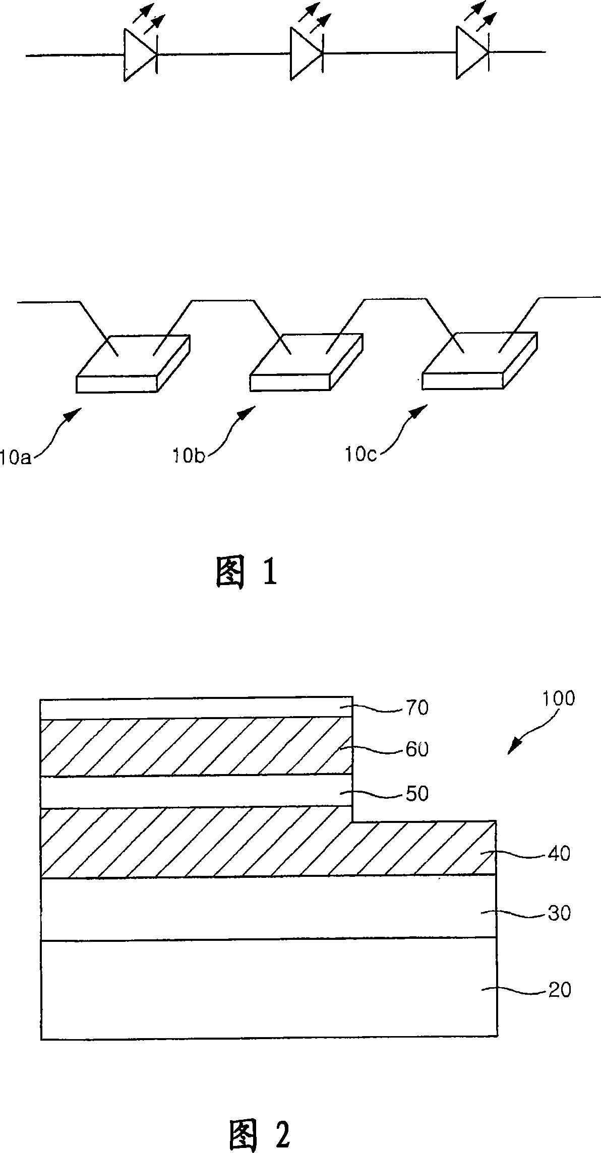
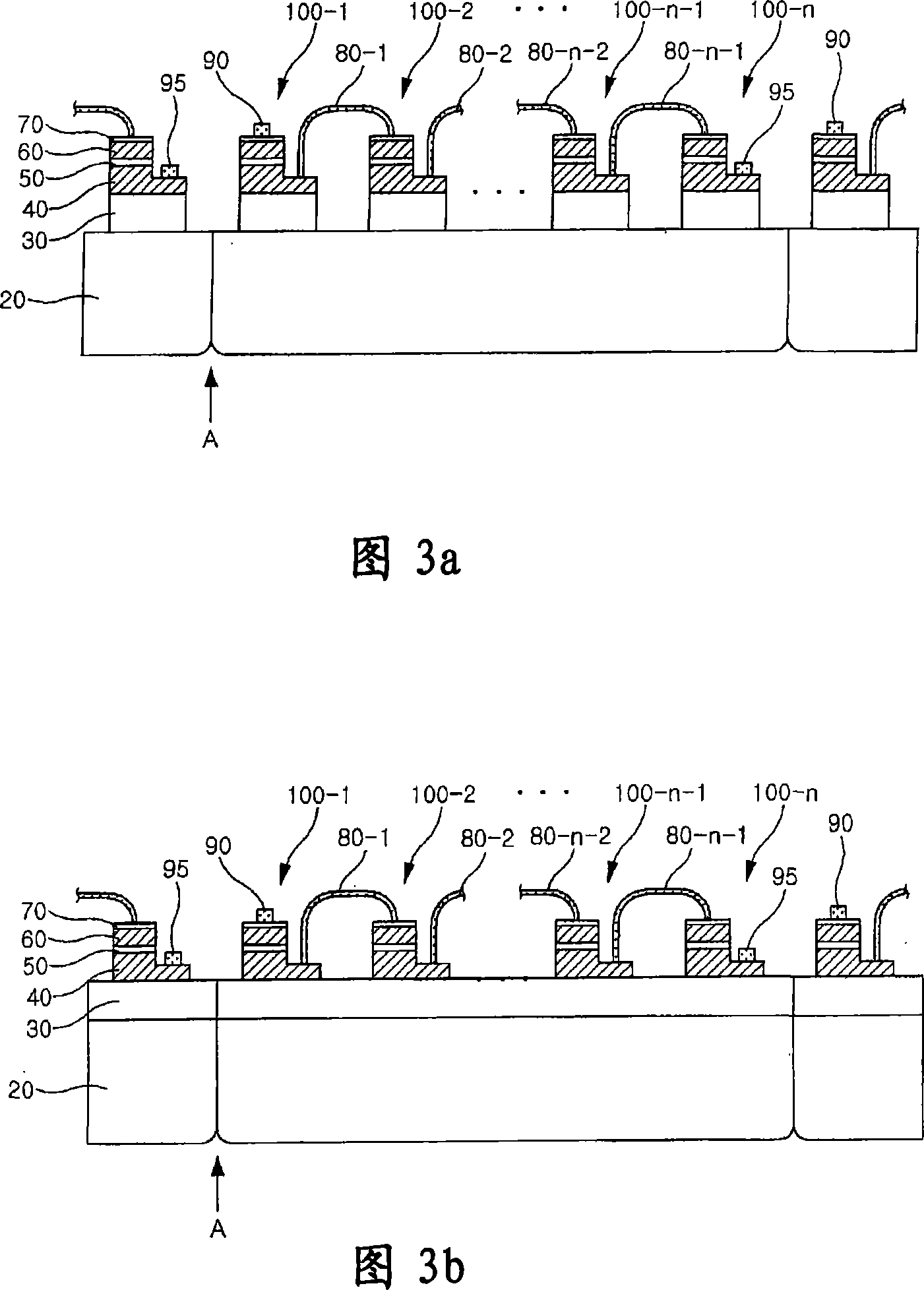
[0036] FIG. 2 is a cross-sectional view of an individual light emitting unit according to an embodiment of the present invention.

[0037] Referring to Fig. 2, light-emitting unit 100 comprises: substrate 20; Buffer layer 30, N-type semiconductor layer 40, active layer 50 and P-type semiconductor layer 60 laminated on substrate 20 sequentially; Formed on N-type semiconductor layer 40 N-type bonding pads (see reference numeral 95 in FIG. 3 a ) on the exposed area of ​​the exposed region; and P-type bondin...


PUM


Abstract

The present invention relates to a light emitting element with arrayed cells, a method of manufacturing the same, and a light emitting device using the same. The present invention provides a light emitting element including a light emitting cell block with a plurality of light emitting cells connected in series or parallel on a single substrate, and a method of manufacturing the same, wherein each of the plurality of light emitting cells includes an N-type semiconductor layer and a P-type semiconductor layer, and the N-type semiconductor layer of one light emitting cell is electrically connected to the P-type semiconductor layer of another adjacent light emitting cell. Further, the present invention provides a light emitting device including a light emitting element with a plurality of light emitting cells connected in series. Accordingly, it is possible to simplify a manufacturing process of a light emitting device for illumination capable of being used with a household AC power source, to decrease a fraction defective occurring in manufacturing a light emitting device for illumination, and to mass-produce the light emitting device for illumination. Further, there is an advantage in that DC driving efficiency can be enhanced in an AC operation by installing a predetermined rectifying circuit outside the light emitting element.

Description

technical field [0001] The present invention relates to a light emitting element incorporating a plurality of units, a method of manufacturing the light emitting element, and a light emitting device using the light emitting element. More specifically, the present invention relates to a single light emitting element having a plurality of light emitting units arrayed on a single substrate, a method of manufacturing the light emitting element, and a light emitting device using the light emitting element. Background technique [0002] A light emitting diode refers to an element that injects minority carriers (electrons or holes) using a p-n junction structure of a semiconductor and recombines certain light emission therethrough. Such light-emitting diodes have been used as display devices and backlights, and research on applying light-emitting diodes to general lighting has been actively conducted. [0003] This is because light emitting diodes have less electric power consumpt...

Claims


Application Information

Patent Timeline
Patent Type & Authority Applications(China)
IPC IPC(8): H01L33/00H01L33/14
CPCY02B20/341H01L2224/48137H01L2224/49107H01L2224/48091H01L2924/00014
Inventor 李贞勋李建宁拉客鲁瓦·伊夫
Owner SEOUL VIOSYS CO LTD
Why Eureka
Try Eureka