Testing method for irradiation of memory and device for implementing method thereof

A test method and memory technology, applied in the direction of single semiconductor device testing, semiconductor/solid-state device testing/measurement, electronic circuit testing, etc., can solve problems such as analysis of difficult critical failure points

Active Publication Date: 2007-08-15
GIGADEVICE SEMICON (BEIJING) INC
View PDF0 Cites 14 Cited by
  • Summary
  • Abstract
  • Description
  • Claims
  • Application Information

AI Technical Summary

Problems solved by technology

With the development of technology, researchers began to place devices with pins biased or not biased or short-circuited under the radiation source for regular irradiation, and then tested an

Method used


Image

  • Testing method for irradiation of memory and device for implementing method thereof

Examples


Embodiment Construction

[0029] The above and other technical features and advantages of the present invention will be described in more detail below in conjunction with the accompanying drawings.

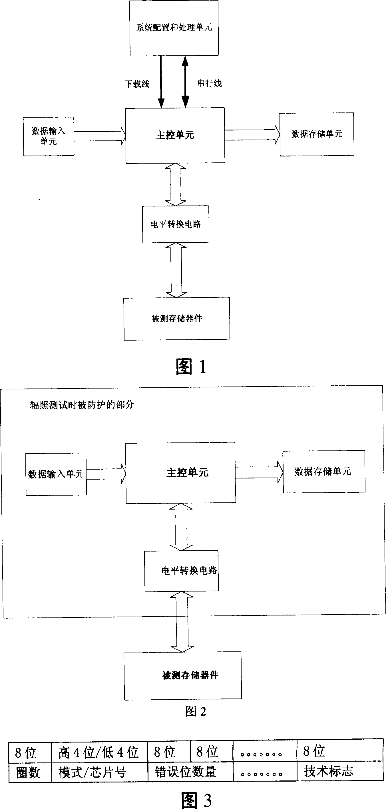
[0030] Since radiation is a cumulative process, the destructiveness it brings shows an upward trend. So in the past, the method of making test records after the radiation was over could not see this phenomenon, and could not fully analyze the destructive power of radiation. Based on the above problems, the present invention proposes a dynamic test method, that is, the device under test can be tested and recorded during the radiation process, so as to more fully understand the damage degree of the radiation process. Its simulation creates a radiation environment. Firstly, the initialization operation is performed, and the specified data is written to all the storage devices under test. Then, the storage devices under test are irradiated with a specified intensity, a specified distance, and a specified time ...


PUM


Abstract

This invention relates to one memory radiation test method and its device, wherein, the device comprises radiation source, level conversion circuit, main control unit, and data input unit and system set and process unit. This invention method comprises the following steps: writing designed data on one memory device; then starting radiation source for memory intensity, set distance, set time; in testing process reading and writing data to the memory part according to read mode; real time comparing the memory part real time output value and predication value to judge whether its is right; once there is wrong data rightly recording its invalid information to find out threshold point of invalid of memory.

Description

technical field [0001] The invention relates to a chip detection technology, in particular to a method and device for dynamically performing radiation testing on storage devices. Background technique [0002] For the current field of memory design, when semiconductor devices are irradiated by high-energy electrons, protons, neutrons or gamma rays, radiation damage will occur. The impact of radiation on the performance of semiconductor materials is mainly related to the ionization and atomic related to displacement. With the improvement of the integration level of integrated circuits and the shrinkage of cell dimensions, radiation effects such as single event effects have become more and more prominent, all of which pose challenges to the application of silicon semiconductor devices. Therefore, it is necessary to conduct irradiation tests on semiconductor devices, test the radiation resistance of integrated circuits, and study the working conditions of integrated circuits in...

Claims


Application Information

Patent Timeline
IPC IPC(8): G01R31/26G01R31/28H01L21/66
Inventor 朱一明韩飞
Owner GIGADEVICE SEMICON (BEIJING) INC
Why Eureka
Try Eureka