
Method for judging leakage current in integrated circuit and MOS element

A technology of oxide semiconductors and integrated circuits, applied in semiconductor/solid-state device testing/measurement, electrical components, circuits, etc., can solve few problems such as integrated circuits, and achieve the effect of shortening feedback time and precise calibration

Active Publication Date: 2007-08-29
TAIWAN SEMICON MFG CO LTD
View PDF0 Cites 11 Cited by
  • Summary
  • Abstract
  • Description
  • Claims
  • Application Information

AI Technical Summary

Problems solved by technology

However, scanning electron microscopy is still mainly used to display images of surface structures, and is rarely used to observe the relevant elements of the internal structure of integrated circuits

Method used


Image

  • Method for judging leakage current in integrated circuit and MOS element
  • Method for judging leakage current in integrated circuit and MOS element
  • Method for judging leakage current in integrated circuit and MOS element

Examples


Embodiment Construction

[0031] In order to make the above and other objects, features and advantages of the present invention more comprehensible, preferred embodiments are listed below and described in detail in conjunction with the accompanying drawings.

[0032] The object of the present invention and its implementation method are described in detail in the following preferred embodiments. However, the concept of the present invention can also be applied in other fields. The following examples are only used to illustrate the purpose and implementation method of the present invention, and are not intended to limit the scope thereof.

[0033] Conventionally, integrated circuits are subjected to wafer-level measurements after wafer fabrication, and the intensity of leakage current is measured during the wafer-level measurements. There is a long delay from the time a possible error handling step (culprit process step) is started to the time a feedback is obtained. Root cause analysis is thus delayed...


PUM

PropertyMeasurementUnit
currentaaaaaaaaaa

Abstract

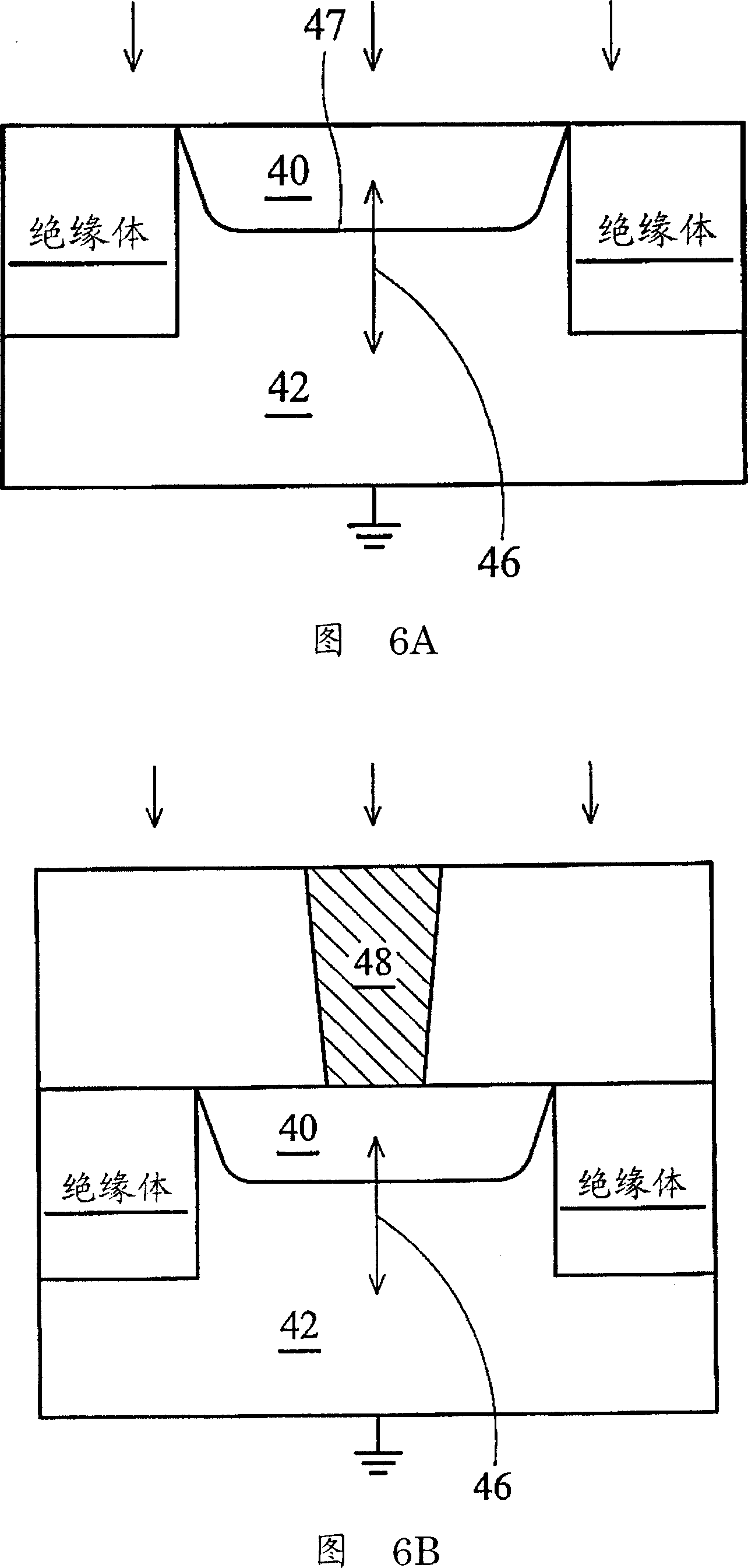
The invention provides a method for judging leakage current in an integrated circuit and a metal oxide semiconductor element. The method includes providing a substrate having a target structure with a first region and a second region. The second zone is first grounded, and then the substrate is scanned using a scanning electron microscope to generate a voltage contrast image. After that, determine the gray scale level of the first interval in the voltage comparison image, and use the gray scale level to determine the leakage current between the first interval and the second interval. The method for judging the leakage current in the integrated circuit and the metal oxide semiconductor element of the present invention can shorten the feedback time for detecting the leakage current, quickly find out the location and intensity of the leakage current, and provide more accurate calibration during the manufacturing process .

Description

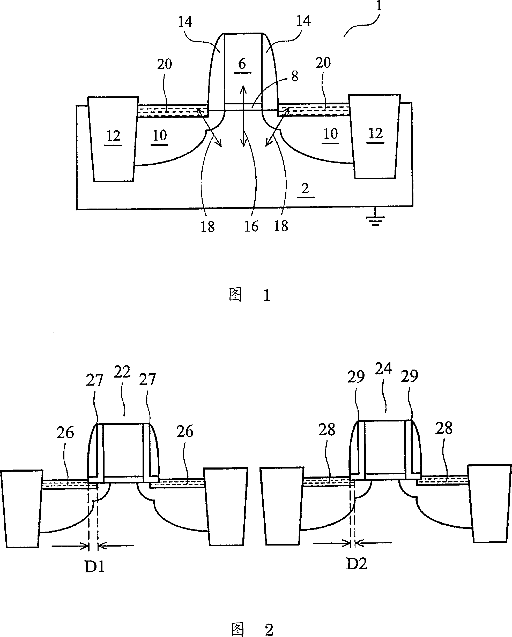
technical field [0001] The invention relates to a method for judging leakage current in integrated circuits and metal oxide semiconductor (MOS) components, in particular to a method for judging leakage current using a scanning electron microscope. Background technique [0002] Scanning electron microscopy (SEM) or electron probe microscopy (EPMA) are microscopic analysis techniques that provide the ability to visualize or analyze materials and distinguish fine objects with visualization techniques. The microscopic capabilities of the above techniques can capture finer objects that cannot be seen even with the aid of an optical microscope, and such resolving capabilities can be used to identify samples composed of elements (such as silicon, iron, etc.). [0003] The scanning electron microscope is used like a camera to shoot the object under test, and its microscopic ability is far superior to that of ordinary optical microscopes. If you shoot in a normal way, the image will...

Claims


Application Information

Patent Timeline
Patent Type & Authority Applications(China)
IPC IPC(8): G01R19/00G01R31/00G01R31/28H01L21/66G01N13/10
CPCH01L22/14G01R31/307
Inventor 陈国香雷明达
Owner TAIWAN SEMICON MFG CO LTD
Learn More