Predictions of leakage modes in integrated circuits

a leakage current and integrated circuit technology, applied in the direction of individual semiconductor device testing, semiconductor/solid-state device testing/measurement, instruments, etc., can solve the problems that few efforts have been concentrated on the research of viewing the characteristics of integrated circuits related to internal structures, and achieve the effect of shortening the feedback time and facilitating rapid identification and modification of culprit processes

Inactive Publication Date: 2008-10-21
TAIWAN SEMICON MFG CO LTD
View PDF2 Cites 3 Cited by
  • Summary
  • Abstract
  • Description
  • Claims
  • Application Information

AI Technical Summary

Benefits of technology

[0010]The preferred embodiments provide a shortened feedback time, so that the culprit processes can be quickly identified and modified. Since the magnitudes of the leakage currents are determined, process adjustment can be performed more precisely.

Problems solved by technology

However, scanning electron microscopes have mainly been used for the imaging of surface structures, and few efforts have been concentrated on the research of viewing the characteristics of the integrated circuits related to the internal structures.

Method used


Image

  • Predictions of leakage modes in integrated circuits
  • Predictions of leakage modes in integrated circuits
  • Predictions of leakage modes in integrated circuits

Examples


Embodiment Construction

[0017]The making and using of the presently preferred embodiments are discussed in detail below. It should be appreciated, however, that the present invention provides many applicable inventive concepts that can be embodied in a wide variety of specific contexts. The specific embodiments discussed are merely illustrative of specific ways to make and use the invention, and do not limit the scope of the invention.

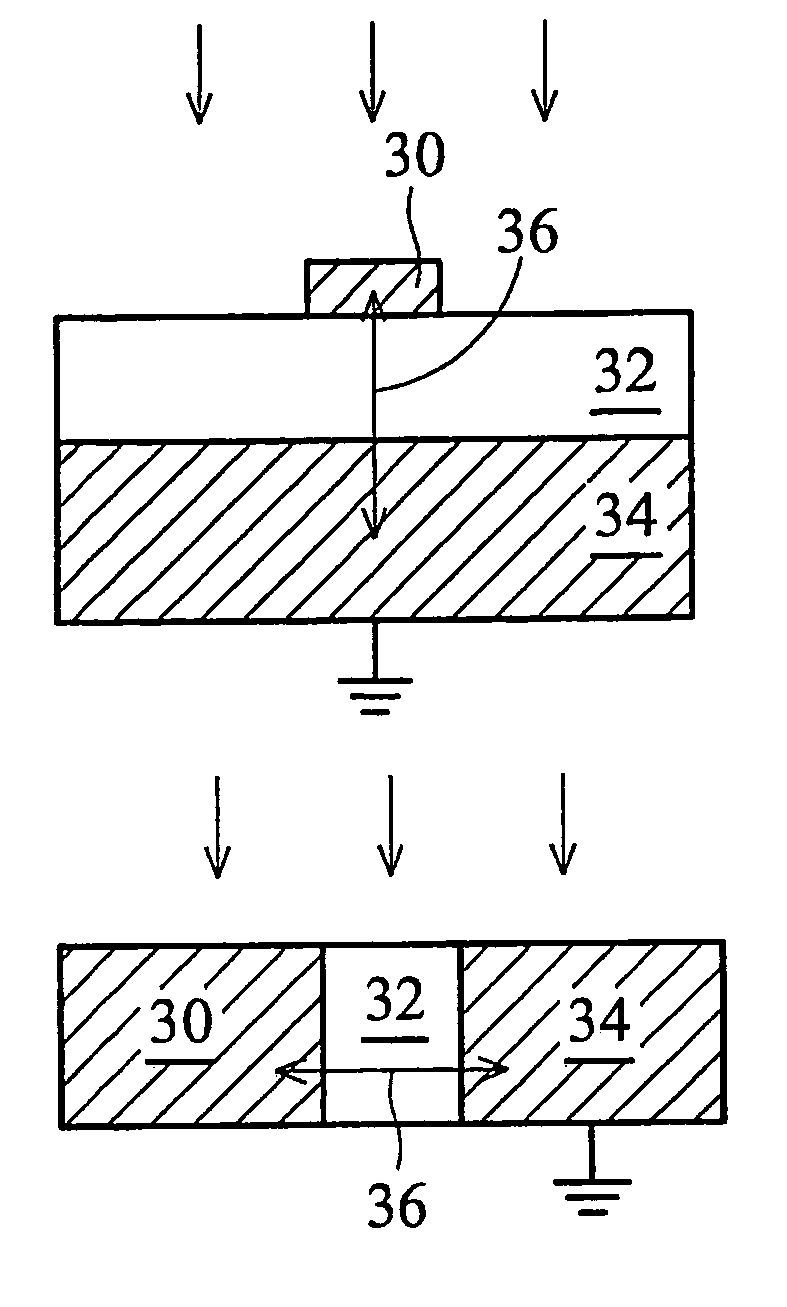
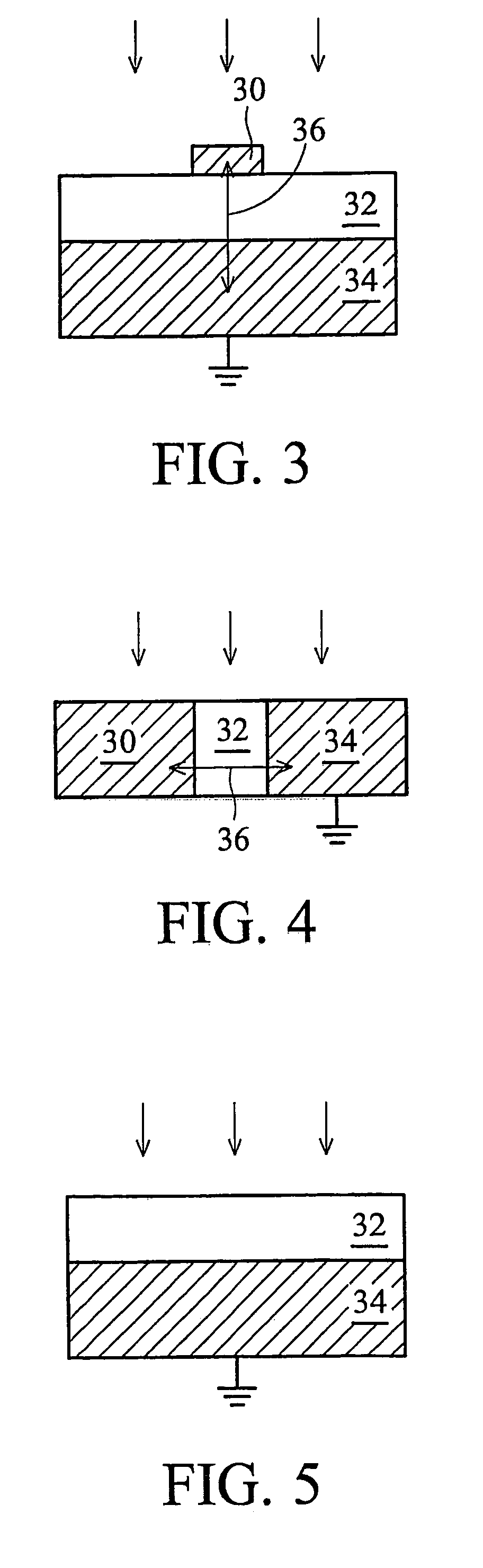
[0018]Conventionally, the magnitudes of leakage currents in integrated circuits are measured through wafer-level measurements, which are performed after the wafers are fabricated. This results in a long time lag from the time when the culprit process step is performed to the time when the feedback is provided. Root cause analysis is thus delayed. To quickly optimize fabrication processes, it is desired that immediately after a feature is fabricated, the leakage current of the feature can be determined.

[0019]The preferred embodiments of the present invention provide a novel me...


PUM


Abstract

A method for determining leakage currents in integrated circuits is provided. The method includes providing a substrate comprising a target structure having a first region and a second region, grounding the second region, scanning the substrate using a scanning electron microscope to produce a voltage contrast (VC) image, determining a gray level of the first region in the VC image, and using the gray level to determine a leakage current between the first region and the second region.

Description

[0001]This application claims priority to provisional patent application Ser. No. 60 / 774,365, filed Feb. 17, 2006, and entitled “Predictions of Leakage Modes in Integrated Circuits,” which application is hereby incorporated herein by reference.TECHNICAL FIELD[0002]This invention relates generally to a method for determining leakage currents in integrated circuits, and more particularly to a method for determining leakage currents using scanning electron microscopy.BACKGROUND[0003]Scanning electron microscopy (SEM) or electron probe microanalysis (EPMA) are micro-analytical techniques, which provide the ability to image or analyze materials that are typically non-observable with the resolution offered by visible techniques. The imaging capability allows for the photographing of an object much smaller than what can be seen even with the aid of an optical microscope, while the analyzing ability allows for the identification of the elements (e.g., silicon, iron, etc.) of which the speci...

Claims


Application Information

Patent Timeline
Patent Type & Authority Patents(United States)
IPC IPC(8): H01L21/66G01R31/26
CPCG01R31/307H01L22/14
Inventor HIANG, TANG KOKLEI, MING-TA
Owner TAIWAN SEMICON MFG CO LTD
Why Eureka
Try Eureka