
High-voltage low-on resistance transmistor with irradiation structure and isolation effect

An on-resistance and transistor technology, applied in the field of lateral double-diffused transistors, can solve problems such as disturbing control signals and control circuit noise interference

Inactive Publication Date: 2007-08-29
SYST GEN
View PDF0 Cites 11 Cited by
  • Summary
  • Abstract
  • Description
  • Claims
  • Application Information

AI Technical Summary

Problems solved by technology

Therefore, noise interference is generated in the control circuit
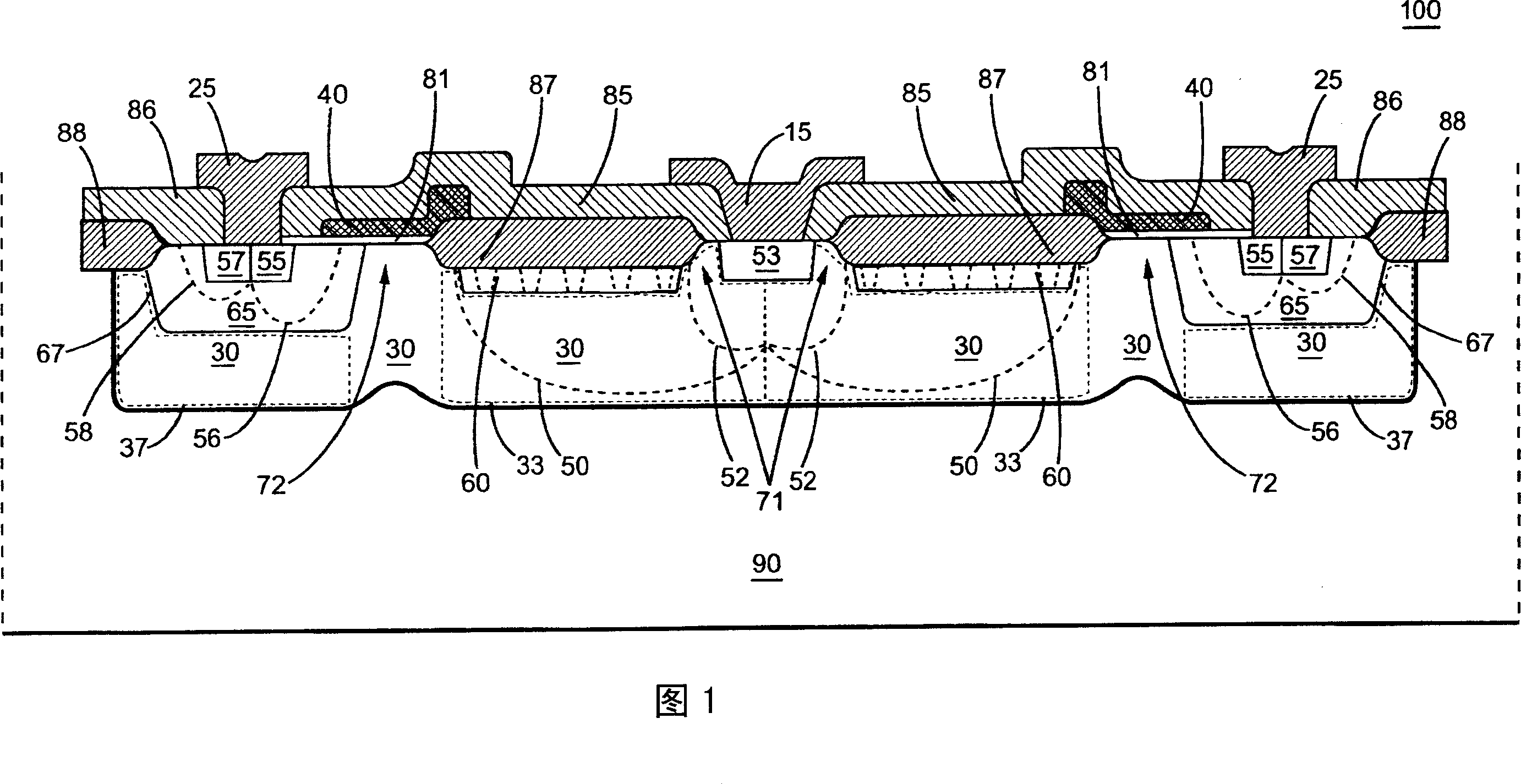
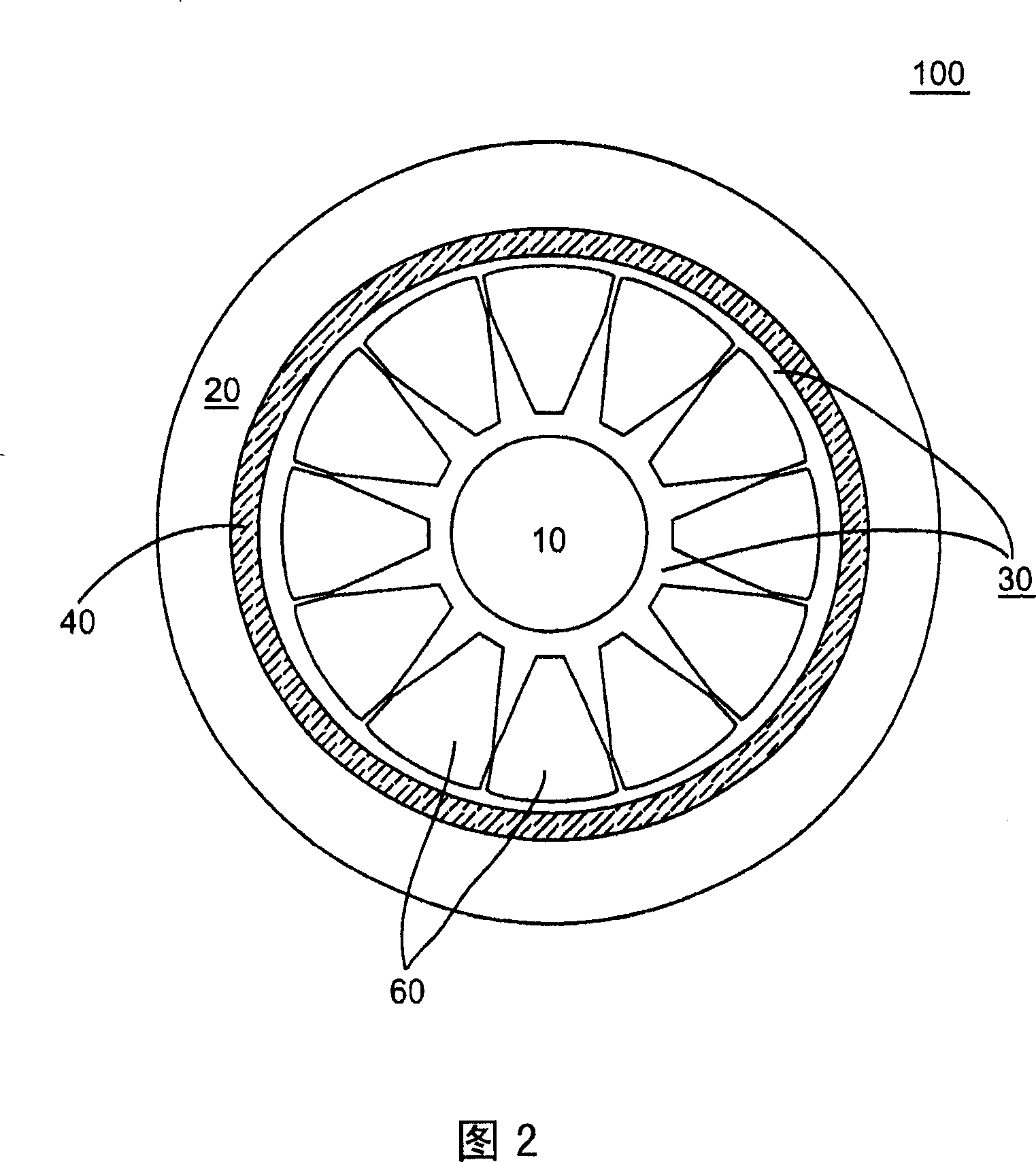
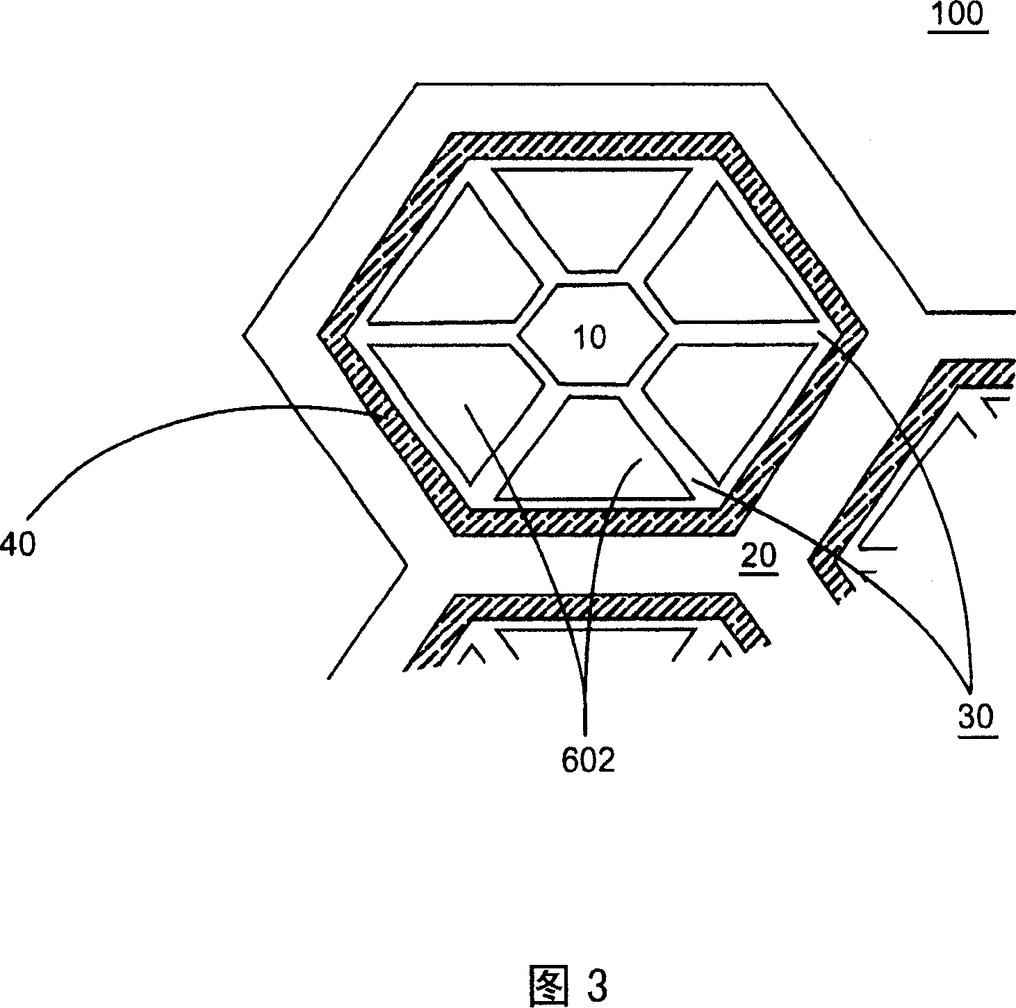
In addition, the current of the LDMOS transistor may generate a ground bounce (ground bounce) that disturbs the control signal

Method used


Image

  • High-voltage low-on resistance transmistor with irradiation structure and isolation effect
  • High-voltage low-on resistance transmistor with irradiation structure and isolation effect
  • High-voltage low-on resistance transmistor with irradiation structure and isolation effect

Examples


Embodiment Construction

[0013] In general, high breakdown voltage transistors do not have a design to isolate each other. In order to improve the isolation effect of the transistor and increase its utilization, the present invention further provides a structure with isolation effect for the high breakdown voltage transistor.

[0014] FIG. 1 is a cross-sectional view of an LDMOS transistor 100 according to the present invention. The LDMOS transistor 100 includes a P-type substrate 90 . The LDMOS transistor 100 further includes a first diffusion region 33 and a second diffusion region 37 containing N-type conductive ions to form an N-type well 30 in the P-type substrate 90 . The first diffusion region 33 includes an extended drain region 50 . A drain diffusion region 53 containing N+ type conductive ions forms a drain region 52 in the extended drain region 50 . A third diffusion region containing P-type conductive ions forms a P-type field block group 60 in the extended drain region 50 . The P-type...


PUM


Abstract

This invention relates to a high voltage and low conductive resistance transistor with a radiation structure and isolation effect, according to that this invented high voltage LDMOS transistor includes at least a P-type field block in the expanded leak region of N-type trap, the P-type field block group forms junctions TI concluded field zone in the N-type trap so as to uniform the capacity values of the parasitic capacitor between the leak and the source regions and hungers the drift region completely before breaking down so as to get a high breakdown voltage and an N-type trap with high doped density, since the source region and the P-type region block surround the leak region, the LDMOS transistor is isolated by itself.

Description

technical field [0001] The present invention relates to a semiconductor device, and in particular to a lateral double-diffusion transistor (LDMOS Transistor) with radiation structure and isolation effect. Background technique [0002] A single-chip process that integrates power switches and control circuits is a major trend in the development of power ICs. Currently, the LDMOS (Lateral Double Diffused MOS) process is especially used in the manufacture of monolithic integrated circuits. The LDMOS process includes planar diffusion on the surface of a semiconductor substrate to form a lateral main current path. [0003] In recent developments, many high voltage LDMOS transistors have been proposed. However, a disadvantage of these prior art LDMOS transistors is their high on-resistance. Therefore, many LDMOS transistors with high voltage and low on-resistance have been proposed one after another. Even so, its complicated production process increases production cost and / or r...

Claims


Application Information

Patent Timeline
IPC IPC(8): H01L27/04H01L29/78
CPCH01L29/0886H01L29/7816H01L29/0696H01L29/0634
Inventor 黄志丰杨大勇林振宇简铎欣
Owner SYST GEN
Learn More