Method for producing high quality silicon single crystal and silicon single crystal wafer made by using the same

A silicon single crystal ingot, high-quality technology, applied in single crystal growth, single crystal growth, chemical instruments and methods, etc., can solve the problems of unstable single crystal growth process, ineffective technology, low production efficiency, etc.

Inactive Publication Date: 2007-09-19
斯尔瑞恩公司
View PDF5 Cites 10 Cited by
  • Summary
  • Abstract
  • Description
  • Claims
  • Application Information

AI Technical Summary

Problems solved by technology

However, this technique requires a temperature holding time of 16 hours or longer, which is only feasible in theory and cannot be applied in practice
[0014] Second, these technologies have no substantive effect
As disclosed in Japanese Patent Application H5-61924 and Eidenzon et al. entitled "Defect-free Silicon Crystals Grown by the Czochralski Technique, Inorganic Materials", Vol.33, No.3, 1997, pp.272-279, it has been tried Growing a 200mm silicon single crystal ingot while periodically changing the crystal pulling speed, but the ideal ...

Method used


Image

  • Method for producing high quality silicon single crystal and silicon single crystal wafer made by using the same
  • Method for producing high quality silicon single crystal and silicon single crystal wafer made by using the same
  • Method for producing high quality silicon single crystal and silicon single crystal wafer made by using the same

Examples


Embodiment Construction

[0037] Preferred embodiments of the present invention will be described in detail below with reference to the accompanying drawings. It should be understood before the description that the terms used in this specification and the appended claims should not be understood as being limited to the general meaning and dictionary meaning, but should be understood based on the meaning and concepts corresponding to the technical aspect of the present invention, and should be understood according to the intention of the inventor Principles for defining terms for best interpretation. Therefore, the description here is only a preferred embodiment for illustrating the purpose, and is not intended to limit the scope of the present invention, so it should be understood that equivalent replacements and changes can be made without departing from the spirit and scope of the present invention .

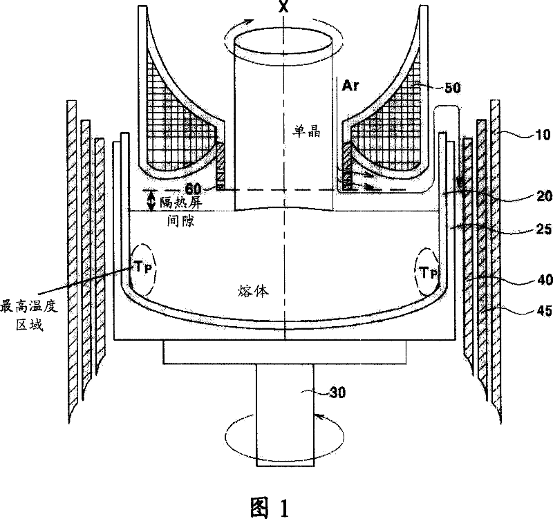
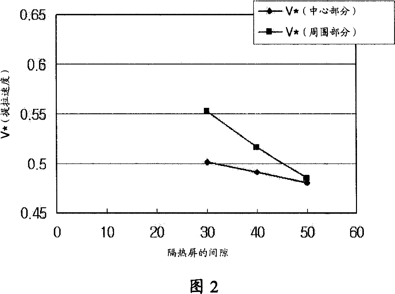
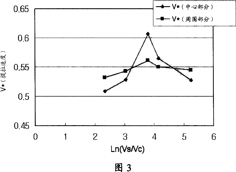
[0038] The present invention is designed based on the fact that controlling the axial temperature ...


PUM


Abstract

In a method for producing a high quality silicon single crystal by the Czochralski method, a lower portion of a solid-liquid interface of a single crystal growth is divided into a central part and a circumferential part, and the temperature gradient of the central part and the temperature gradient of the circumferential part are separately controlled. When a silicon melt located at a lower portion of a solid-liquid interface of a single crystal growth is divided into a central part melt and a circumferential part melt, the method controls the temperature gradient of the central part melt by directly controlling the temperature distribution of a melt and indirectly controls the temperature gradient of the circumferential part melt by controlling the temperature gradient of the single crystal, thereby effectively controlling the overall temperature distribution of the melt, thus producing a high quality single crystal ingot free of defects with a high growth velocity.

Description

technical field [0001] The present invention relates to a method for manufacturing a high-quality silicon single-crystal ingot free from point defects, and more particularly to a method for manufacturing a high-quality silicon single-crystal ingot, wherein when growing a silicon single-crystal ingot by the Czochralski method (Czochralski method), by controlling The temperature profile of the melt is used to control growth defects. Background technique [0002] In order to grow a high-quality silicon single crystal ingot capable of increasing the yield of semiconductor devices, conventional techniques control the temperature distribution of the high temperature region of the single crystal ingot after crystallization. This is to control stress caused by shrinkage due to cooling after crystallization, or to control movement of point defects occurring during crystallization. [0003] In general, the method of manufacturing silicon single crystal ingots by the Czochralski metho...

Claims


Application Information

Patent Timeline
IPC IPC(8): C30B29/06C30B15/20
CPCC30B15/10C30B15/203C30B15/206C30B15/30C30B29/06H01L21/02002
Inventor 赵铉鼎
Owner 斯尔瑞恩公司
Why Eureka
Try Eureka