Pattern forming method and gray-tone mask manufacturing method

A manufacturing method and a grayscale mask technology, which are applied in the photolithographic process of the pattern surface, semiconductor/solid-state device manufacturing, and originals for photomechanical processing, etc., can solve the problem of difficult detection of alignment marks, positional deviations, Low detection accuracy and other problems, to achieve the effect of good detection accuracy and increased contrast

Inactive Publication Date: 2007-09-19
HOYA CORP
View PDF1 Cites 7 Cited by
  • Summary
  • Abstract
  • Description
  • Claims
  • Application Information

AI Technical Summary

Problems solved by technology

However, in the above-mentioned pattern drawing process, when the alignment mark composed of the light-shielding portion and the light-transmitting portion is detected by reflected light, if an anti-reflection film is formed on the uppermost layer of the light-shielding portion of the alignment mark, then due to The difference in reflectance from the glass substrate surface of the light-transmitting part of the alignment mark is small, and the contrast of reflection cannot be obtained, so it is difficult to detect the alignment mark
When the detection accuracy of the alignment mark is low, the first drawing pattern and the second drawing pattern cannot be aligned with high precision, which causes positional deviation between the first drawing pattern and the second drawing pattern
When manufacturing, for example, a TFT substrate using a grayscale mask on which a device pattern with a positional deviation is formed, a serious failure (operation failure) may occur

Method used


Image

  • Pattern forming method and gray-tone mask manufacturing method
  • Pattern forming method and gray-tone mask manufacturing method
  • Pattern forming method and gray-tone mask manufacturing method

Examples


Embodiment 1

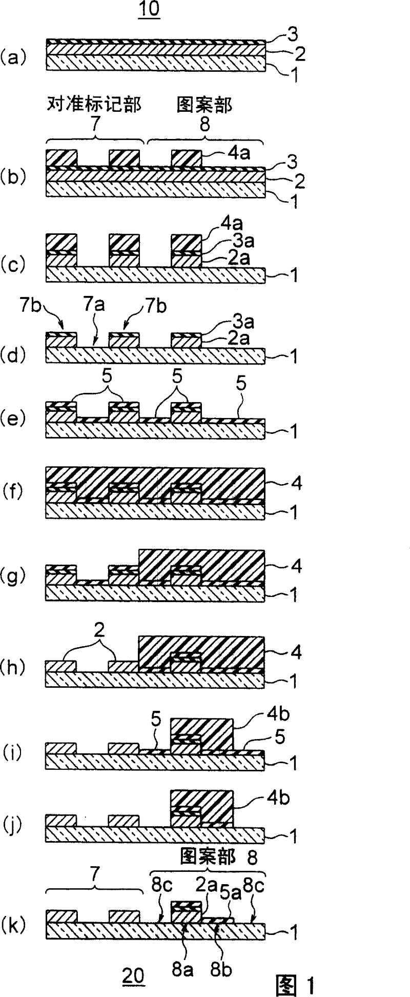
[0042] 1 shows an embodiment 1 in which the pattern forming method of the present invention is applied to the manufacturing process of a gray scale mask formed on a translucent substrate with The device pattern of the light-shielding part, the light-transmitting part and the semi-transparent part.

[0043] As shown in FIG. 1( a ), the mask blank 10 used in this example has a light-shielding film 2 and an antireflection film 3 formed on a light-transmitting substrate 1 such as synthetic quartz glass. Here, as the material of the light-shielding film 2 , a material capable of obtaining high light-shielding properties as a thin film is preferable, and examples thereof include Cr, Si, W, Al, and the like. Moreover, as a material of the antireflection film 3, oxide etc. which are mentioned above-mentioned light-shielding layer materials are mentioned, for example.

[0044] The mask blank 10 described above can be obtained by sequentially forming a light-shielding film 2 and an ant...

Embodiment 2

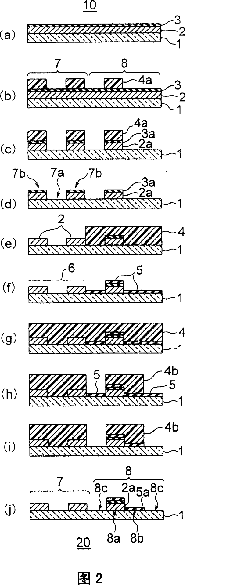
[0062] FIG. 2 is a schematic cross-sectional view showing Example 2 in which the pattern forming method of the present invention is applied to a manufacturing process of a gray scale mask.

[0063] 2( a ) to FIG. 2( d ) are completely the same as those in FIG. 1( a ) to FIG. 1( d ) in the first embodiment.

[0064] Next, as shown in FIG. 2( e ), a resist film 4 is formed on a portion other than the alignment mark 7 . As a method of forming the resist film 4 on the portion other than the alignment mark 7, after forming the resist film on the entire surface as described in Example 1, removing or removing the alignment mark 7 by spot exposure or development can be used. part, or a method of applying a resist to a part other than the alignment mark 7, etc. Then, the antireflection film 3 located on the surface of the light shielding portion 7b of the alignment mark 7 is removed by etching.

[0065] Next, as shown in FIG. 2( f ), the part of the alignment mark 7 is protected by a...

Embodiment 3

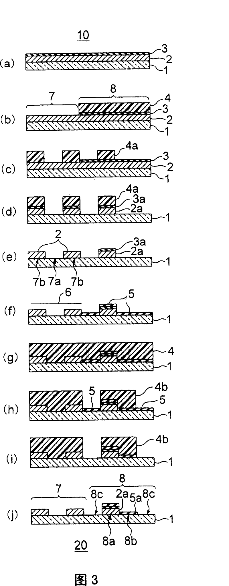
[0070] 3 is a schematic cross-sectional view showing Example 3 in which the pattern forming method of the present invention is applied to a manufacturing process of a gray scale mask.

[0071] As shown in Fig. 3(a) and Fig. 3(b), in this embodiment, a resist film 4 is formed on the region of the mask blank 10 except for the alignment mark 7, and the alignment mark 7 is removed by etching or the like. The anti-reflection film 3 of the portion marked 7 .

[0072] Next, as shown in FIG. 3( c), after peeling off the remaining resist film 4, a resist film is formed on the entire surface again, and pattern drawing including the alignment mark 7 and the first pattern is performed in the same manner as in Example 1. , and developed to form a resist pattern 4a. Next, as shown in FIG. 3( d ), by using the resist layer pattern 4 a as a mask, the exposed light-shielding film 2 is etched to remove the remaining resist layer pattern 4 a, thereby forming the resist layer pattern 4 a shown i...


PUM


Abstract

The invention provides a method for forming pattern, has plural pattern forming processes using photoetching process. The processes for forming same substrate at least has: A process for forming alignment mark used for depicting alignment; and a process for depicting pattern by using the alignment mark for alignment, wherein the alignment mark is comprised by lightproof portion and translucent portion, and before depicting the pattern, the reflection proof membrane of the lightproof portion of the alignment mark which has the reflection proof membrane on top layer is eliminated.

Description

technical field [0001] The present invention relates to preferred patterns in the manufacture of grayscale masks used in the manufacture of liquid crystal displays (Liquid Crystal Display: hereinafter referred to as LCD) and the like, and phase shift masks used in the manufacture of semiconductors. form method. Background technique [0002] Conventionally, in the field of LCDs, a method of reducing the number of photomasks (photo masks) required for manufacturing has been proposed. That is, thin film transistor liquid crystal display (Thin Film Transistor Liquid Crystal Display: hereinafter referred to as TFT-LCD) has the advantages of easy thinning and low power consumption compared with CRT (cathode line tube), so it is currently moving towards commercial products. rapid development. TFT-LCD has the following schematic structure, that is, a TFT substrate with a structure in which TFTs are arranged in each pixel arranged in a matrix, and color filters in which red, green,...

Claims


Application Information

Patent Timeline
Patent Type & Authority Applications(China)
IPC IPC(8): G03F7/20G03F1/14H01L21/027G03F1/42
CPCG03F1/36G03F1/38G03F9/708
Inventor 佐野道明元村秀峰
Owner HOYA CORP
Why Eureka
Try Eureka