Organic light emitting devices comprising dielectric capping layers

A technology for organic light-emitting devices and covering layers, which is applied in the direction of electric solid devices, electrical components, semiconductor devices, etc., can solve the problems of low contrast ratio of organic LEDs, difficult to handle manufacturing methods, and complex displays.

Active Publication Date: 2007-09-26
IBM CORP
View PDF1 Cites 18 Cited by
  • Summary
  • Abstract
  • Description
  • Claims
  • Application Information

AI Technical Summary

Problems solved by technology

This leads to a complex and intractable manufacturing method for displays comprising multiple organic LEDs, ie a separate process step is necessary for each thickness of the refractive dielectric layer 208
[0012] ...

Method used


Image

  • Organic light emitting devices comprising dielectric capping layers
  • Organic light emitting devices comprising dielectric capping layers
  • Organic light emitting devices comprising dielectric capping layers

Examples


Embodiment Construction

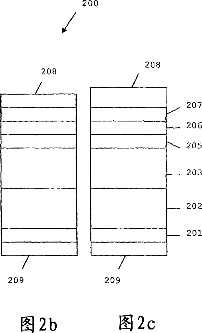
[0049] Figures 3a-c show schematic diagrams of an array of three sub-pixels constituting an organic light emitting device (OLED). In an embodiment of the invention the organic light emitting device is an organic light emitting diode. Each OLED of array 300 includes a substrate 309 . In the illustrated embodiment, substrate 309 is a glass substrate on which indium tin oxide (ITO) layer 301 is formed. Under the glass substrate 309, ie, opposite to the ITO layer 301, a mirror layer 310 is formed. The ITO layer 301 serves as a first electrode such as an anode of the organic light emitting diode, and is connected to a power source not shown in FIG. 3 . A mirror layer 310 is formed to increase the efficiency of the OLED. Such a mirror layer 310 may be formed, for example, by a silver layer or a dielectric material.

[0050] Alternatively, an aluminum layer may be used to form the anode 301 . In this case, the mirror layer 310 can be formed by treating the aluminum layer of the ...


PUM


Abstract

The present invention is directed to an organic light emitting device comprising a multilayer structure with a first electrode, a second electrode, at least one layer of organic material, arranged between said first electrode and said second electrode, and a dielectric capping layer, arranged on said second electrode opposite to said first electrode, wherein said capping layer comprises an outer surface, opposite to said second electrode, for emission of light generated in said at least one layer of organic material. The capping layer has the effect that a reflectance of external light is reduced whereas outcoupling of the light generated in the at least one layer of organic material through said capping layer is increased.

Description

technical field [0001] The present invention provides an organic light emitting device, a manufacturing method thereof, and an array including a plurality of organic light emitting devices. Background technique [0002] In recent years, mobile information and telecommunication devices such as notebook computers and personal digital assistants have undergone rapid development. Corresponding devices are becoming ever lighter and more efficient. Currently flat panel displays are becoming more and more common for such devices. Today, so-called liquid crystal displays (LCDs) are used as flat panel displays, although LCDs have certain disadvantages such as the need for a backlight and a limited viewing angle. [0003] In addition to liquid crystals, organic light-emitting diodes, so-called organic LEDs or OLEDs, can also be used in flat panel displays. Such organic LEDs have higher luminous efficiency and increased viewing angles. The fundamental feature of organic LEDs is the...

Claims


Application Information

Patent Timeline
IPC IPC(8): H01L51/52
CPCH01L51/5262H01L51/5237H01L51/5221H01L51/5281H10K50/826H10K50/85H10K50/844H10K50/858H10K50/86H10K50/82H10K50/856H10K50/84
Inventor 西格弗里德·F.·卡格沃尔特·雷斯海克·E.·雷尔康斯坦斯·罗斯特中村肇
Owner IBM CORP
Why Eureka
Try Eureka