Pattern defect inspection method, photomask manufacturing method, and display device substrate manufacturing method
一种缺陷检查、制造方法的技术,应用在测量装置、图纹面的照相制版工艺、半导体/固态器件制造等方向,能够解决检查结果改变等问题,达到提高生产率的效果
- Summary
- Abstract
- Description
- Claims
- Application Information
AI Technical Summary
Problems solved by technology
Method used
Image
Examples
no. 1 example
[0056] [A] First Embodiment (FIGS. 1 to 7B)
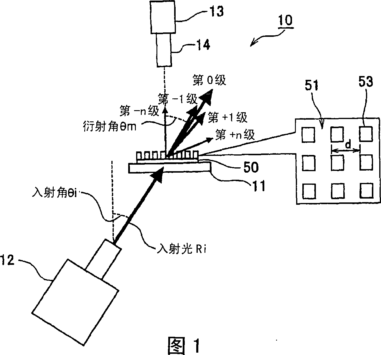
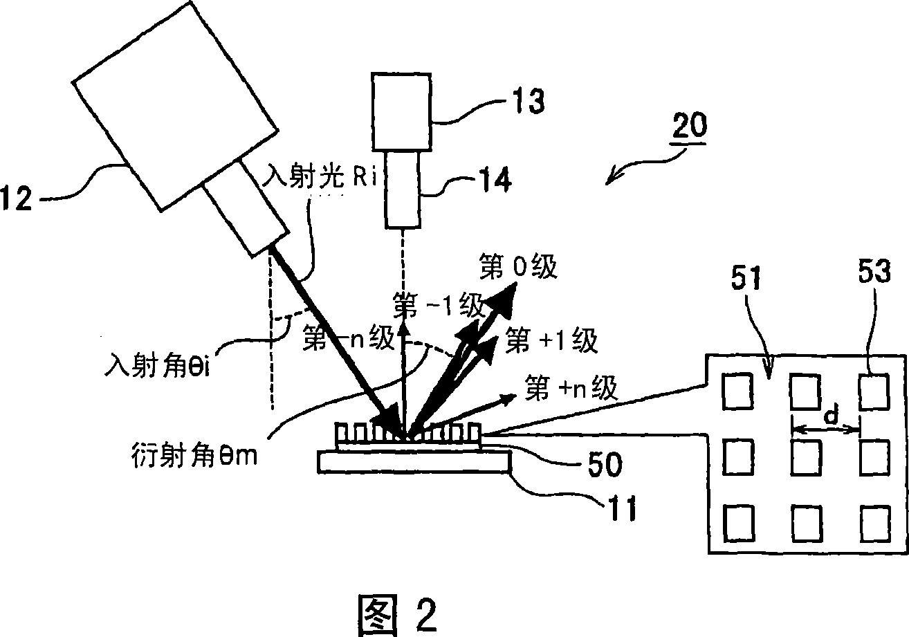
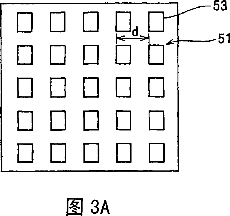
[0057] FIG. 1 is a schematic side view showing a defect inspection apparatus for performing a defect inspection method according to a first embodiment of the present invention. FIG. 2 is a schematic side view showing a modified example of the defect inspection apparatus shown in FIG. 1 . 5 is a plan view showing a photomask to be inspected as an inspection object in the defect inspection method shown in FIGS. 1 and 2 .
[0058] As shown in FIG. 5, in the defect inspection method of this embodiment, a photomask 50 to be inspected as an inspection object is an exposure mask for manufacturing a substrate such as a liquid crystal display (in particular, a flat panel). Display: Display device of FPD), plasma display, EL display, LED display or DMD display.
[0059] The photomask 50 includes a transparent substrate such as a synthetic quartz glass substrate and a thin film (light shielding film) such as a chromium film formed on the su...
no. 2 example
[0094] [B] Second Embodiment (FIG. 8)
[0095] 8 is a side sectional view showing a photomask to be inspected in a defect inspection method of a second embodiment of the present invention. The second embodiment is different from the first embodiment described above in that the defect inspection process is performed after the resist pattern forming process, and thereafter, the process of removing the resist pattern for the auxiliary pattern 57 and forming the mask are performed in a specified order. The process of molding the pattern (ie, the thin film pattern of the main pattern 56).
[0096] That is, in the resist pattern forming process, the resist patterns 61 and 62 for forming the main pattern 56 and the auxiliary pattern 57 are respectively written on the thin film 60 formed on the surface of the transparent substrate 59 using a writing device according to a grating writing technique. formed on the resist film and then developed.
[0097] In the defect inspection proces...
no. 3 example
[0103] The auxiliary pattern removal process of the pattern defect inspection method according to the third embodiment is different from the second embodiment described above.
[0104] That is, in this third embodiment, etching is performed after defect inspection using the resist pattern 62 for the auxiliary pattern 57 to form a thin film pattern of the main pattern 56 (ie, the main pattern 56 in the first embodiment) and a thin film pattern of the auxiliary pattern 57 (ie, the auxiliary pattern 57 in the first embodiment), and then strip the resist, thereby manufacturing a temporary photomask.
[0105] Thereafter, a resist is coated again on the entire surface of the temporary photomask, and then only a portion of the resist corresponding to the auxiliary pattern 57 is exposed. The exposure may be scanning exposure by a scribing device, or surface exposure only at such a portion. Development is performed again after exposure, and then etching is performed again, thereby rem...
PUM
 Abstract
Description
Claims
Application Information


