Supercharge Your Innovation With Domain-Expert AI Agents!

A semiconductor memory part and its making method

A technology of storage devices and manufacturing methods, which is applied in semiconductor/solid-state device manufacturing, semiconductor devices, electric solid-state devices, etc., and can solve the problems of expensive manufacturing of memory devices and high barriers to entry

Active Publication Date: 2007-11-28
GIGADEVICE SEMICON (BEIJING) INC
View PDF0 Cites 0 Cited by
  • Summary
  • Abstract
  • Description
  • Claims
  • Application Information

AI Technical Summary

Problems solved by technology

As a result, memory devices are more expensive to manufacture and any specialized process may require an entirely new foundry, making the barrier to entry higher

Method used


Image

  • A semiconductor memory part and its making method
  • A semiconductor memory part and its making method
  • A semiconductor memory part and its making method

Examples


Embodiment Construction

[0046] The invention will be described in detail below with reference to preferred embodiments illustrated in the accompanying drawings. In the course of description, the present invention has been set forth in detail and precisely for a thorough understanding of the present invention. It will be apparent, however, to one skilled in the art that the present invention may be practiced without some or all of these specific details. In order to avoid unnecessarily obscuring the description of the present invention, some well known process steps or structures may not be described in detail.

[0047] Embodiments of the present invention relate to semiconductor memory devices, and more particularly to semiconductor memory devices and structures thereof that provide high-efficiency manufacturing and functionality of memory by using a preferred logic manufacturing process.

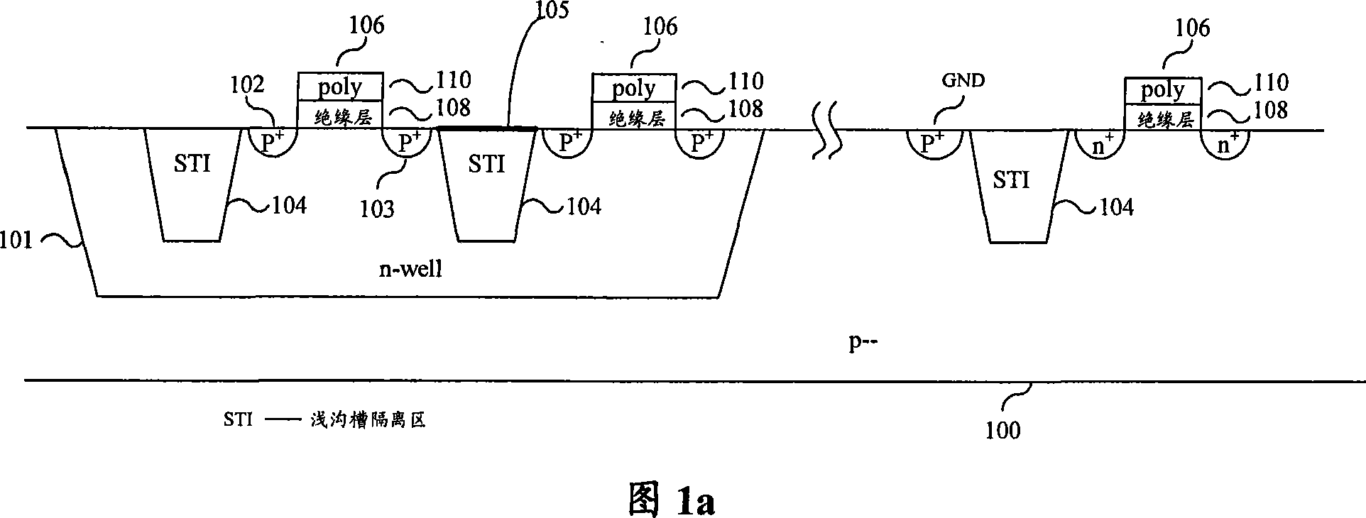
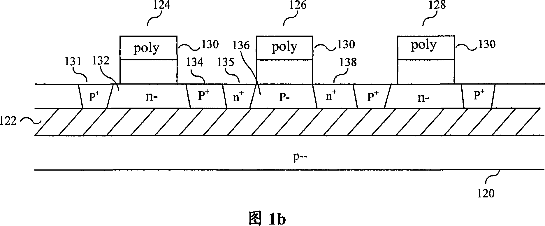
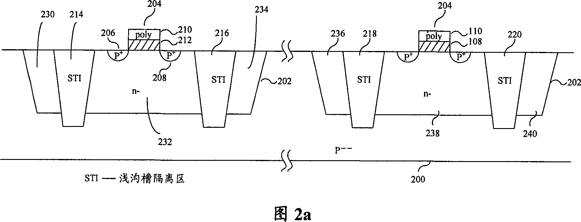
[0048] Referring to Figure 2a, there is illustrated a presently preferred embodiment of the present invention ...


PUM


Abstract

The invention discloses a semiconductor storing element, which comprises the following parts: substrate, first cavity in the substrate, active element on the first cavity, and one or more grooves with depth more than the depth of the first cavity. The invention also provides the making method of semiconductor storage, which comprises the following steps: forming the first cavity in the substrate; forming the active element on the first cavity; forming one or more separating grooves with depth more than the depth of the first cavity. The invention reserves information in the memory, which reduces the manufacturing cost and power consumption greatly with small area for storage element.

Description

technical field [0001] The present invention relates to a semiconductor storage device, in particular to a semiconductor storage device manufactured using a standard process and a manufacturing method thereof. Background technique [0002] In the fabrication of semiconductor memory devices, a widely used and cost-effective fabrication process offered by many fabs is the standard process, the bulk complementary metal-oxide-semiconductor (CMOS) process. In the standard manufacturing process of semiconductor devices, referring to FIG. 1a as an example, a p-type bulk silicon substrate 100 can be placed on which one or more n-type wells 101 can be placed. One way to electrically isolate active device regions within well 101 is to form trench isolation regions 104 between adjacent devices 106 . Such prior art trench isolation regions typically comprise formed in the substrate and are made of such as silicon dioxide (SiO 2 ) trenches filled with dielectric material. Active devic...

Claims


Application Information

Patent Timeline
Patent Type & Authority Applications(China)
IPC IPC(8): H01L27/10H01L21/822H01L21/76
Inventor 朱一明
Owner GIGADEVICE SEMICON (BEIJING) INC
Features
  • R&D
  • Intellectual Property
  • Life Sciences
  • Materials
  • Tech Scout
  • Unparalleled Data Quality
  • Higher Quality Content
  • 60% Fewer Hallucinations
Learn More