

Light emission microscope opposite side sample fixer
A light emission microscope, sample fixation technology, applied in microscopes, optics, instruments, etc., can solve the problems of difficulty in analysis, air bubbles on the back of the chip and glass, and pollution on the chip surface, and achieves the effect of easy use, avoidance of waste, and avoidance of pollution.
- Summary
- Abstract
- Description
- Claims
- Application Information
AI Technical Summary
Problems solved by technology
Method used
Image

Examples
Embodiment 1
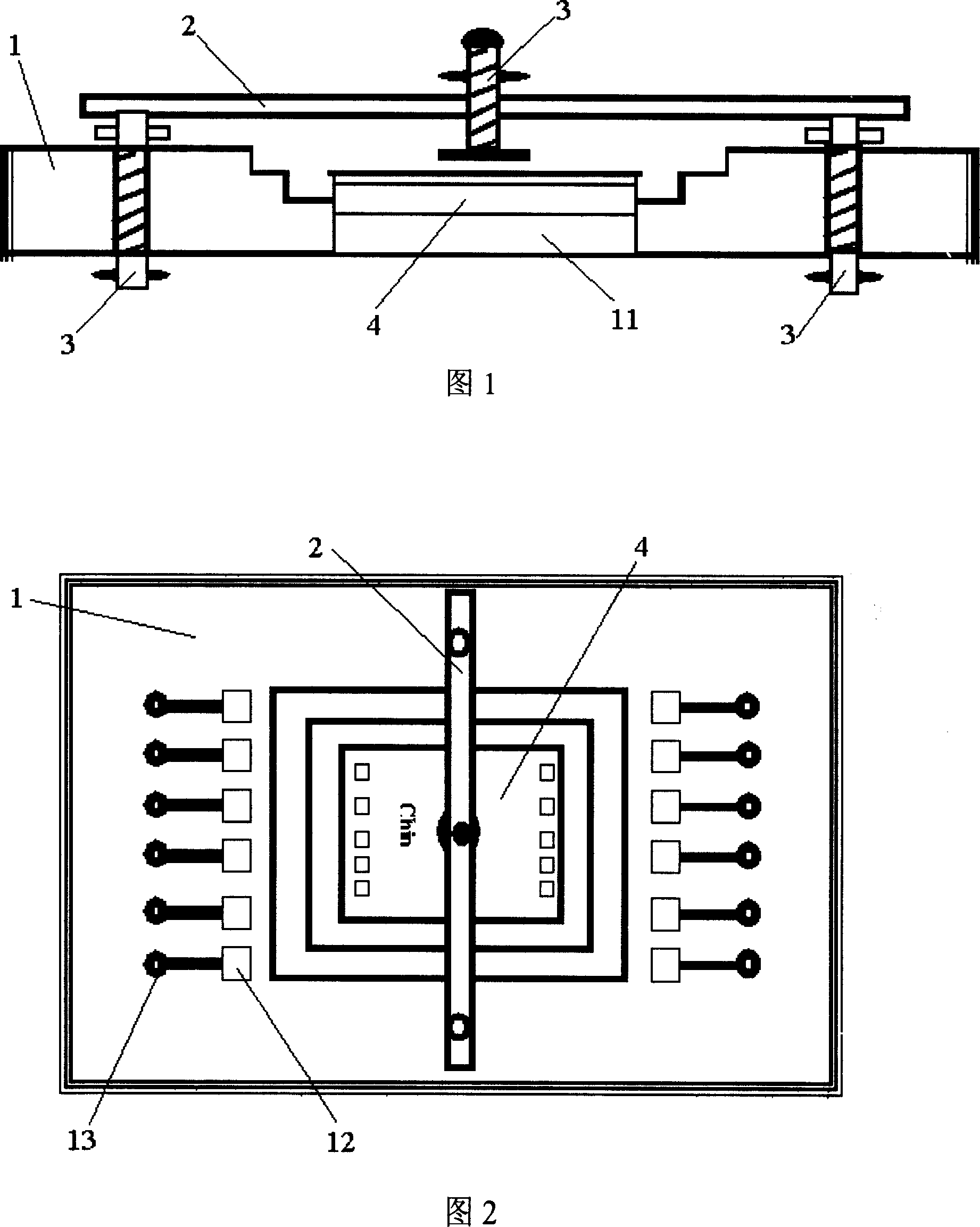
[0036] Fig. 1 shows the sectional view of the sample holder on the back of the light emission microscope of the present invention, which has the following structure: a sample carrying substrate 1, a sample fixing rod 2 and at least three movable threaded gaskets 3;
[0037] A light-transmitting glass sheet 11 is inlaid in the center of the sample carrying substrate as a position for carrying the sample chip 4;
[0038] Both ends of the sample fixing rod 2 are respectively connected to both sides of the sample carrying substrate 1 by movable threaded gaskets 3;
[0039] Among the at least three movable threaded gaskets 3, at least two movable threaded gaskets 3 are penetrated on both sides of the sample carrying substrate 1, and are respectively fixed to the two ends of the sample fixing rod 2, at least one of which can be The moving thread gasket 3 is installed in the middle of the sample fixing rod 2 .
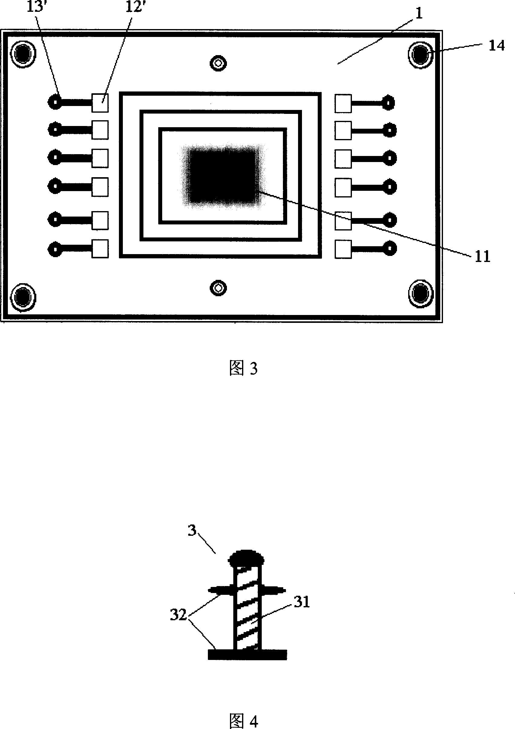
[0040] The specific structure of the above-mentioned sample carrier sub...
PUM
 Abstract
Description
Claims
Application Information