Array substrate for liquid crystal display device and method of fabricating the same

A liquid crystal display and array substrate technology, applied in semiconductor/solid-state device manufacturing, static indicators, instruments, etc., can solve problems such as increased brightness of dark images, voltage drop, and increased resistance of the common line 40

Inactive Publication Date: 2008-01-02
LG PHILIPS LCD CO LTD
View PDF1 Cites 18 Cited by
  • Summary
  • Abstract
  • Description
  • Claims
  • Application Information

AI Technical Summary

Problems solved by technology

As a result, the brightness of dark images increases, resulting in a decrease in the aperture ratio
[0017] In addition, if the aperture ratio is increased by reducing the width of the common line 40 in the pixel region "P", the resistance of the common line 40 increases, which will cause a voltage drop
On the other hand, when the width of the common line increases, the supplied storage voltage becomes unstable and the aperture ratio decreases

Method used


Image

  • Array substrate for liquid crystal display device and method of fabricating the same
  • Array substrate for liquid crystal display device and method of fabricating the same
  • Array substrate for liquid crystal display device and method of fabricating the same

Examples


Embodiment Construction

[0034] Preferred exemplary embodiments will be described in detail with reference to examples illustrated in the accompanying drawings.

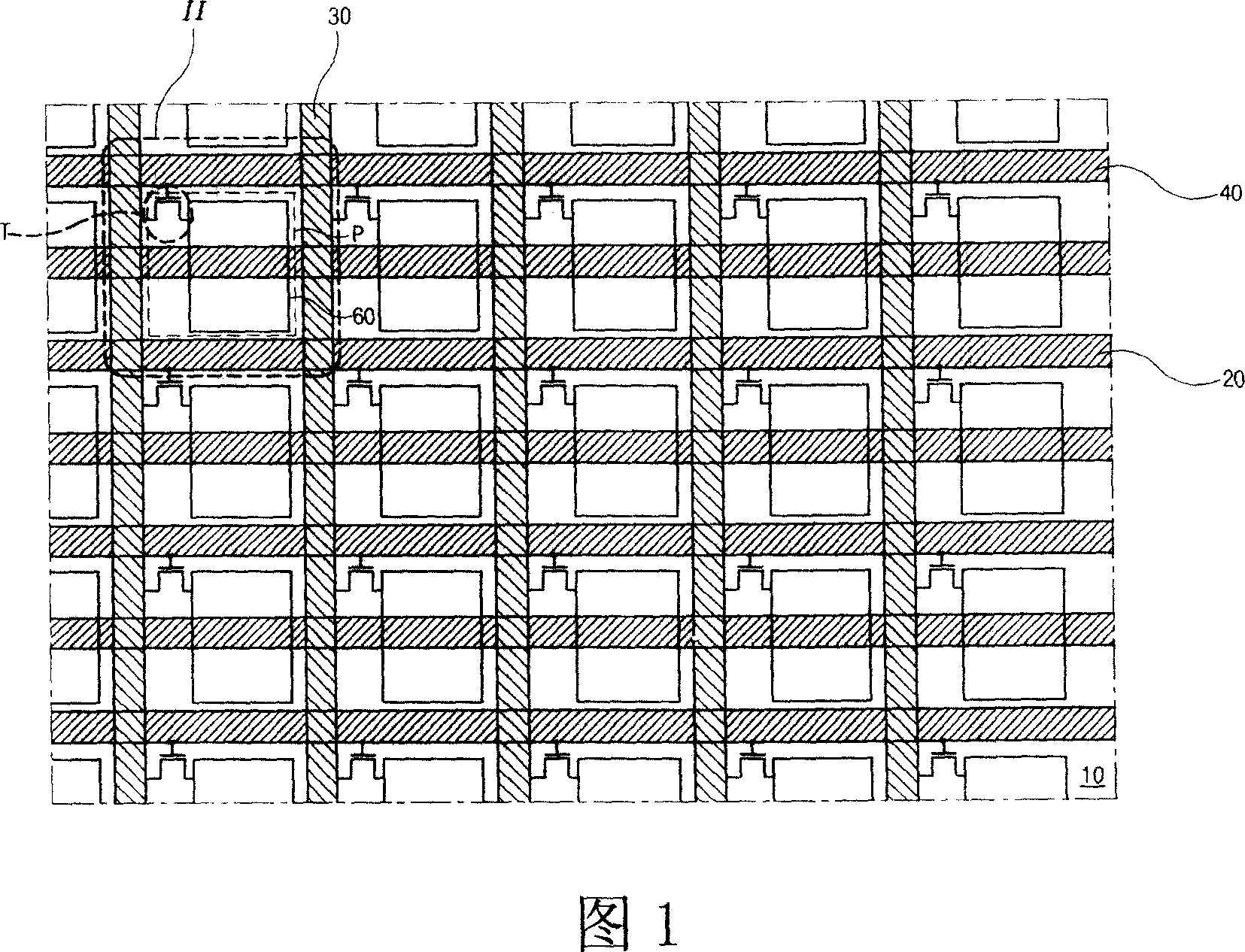
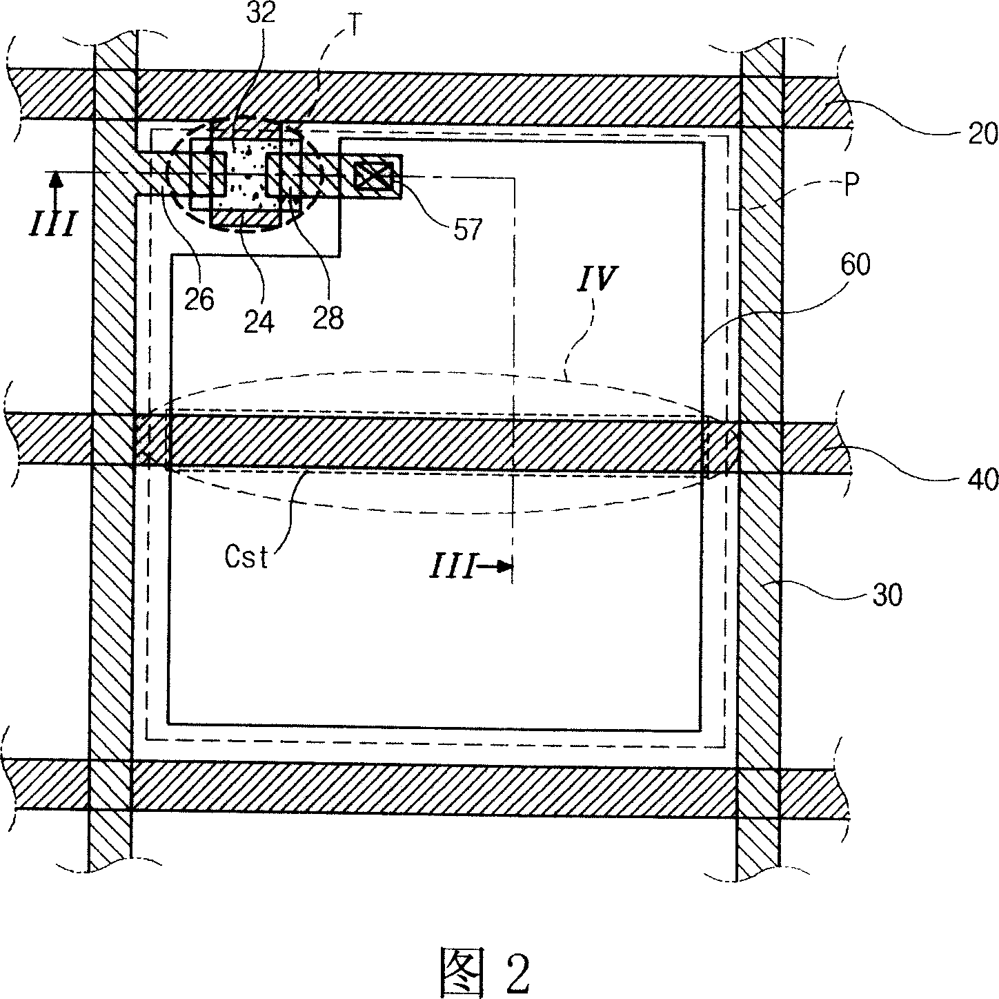
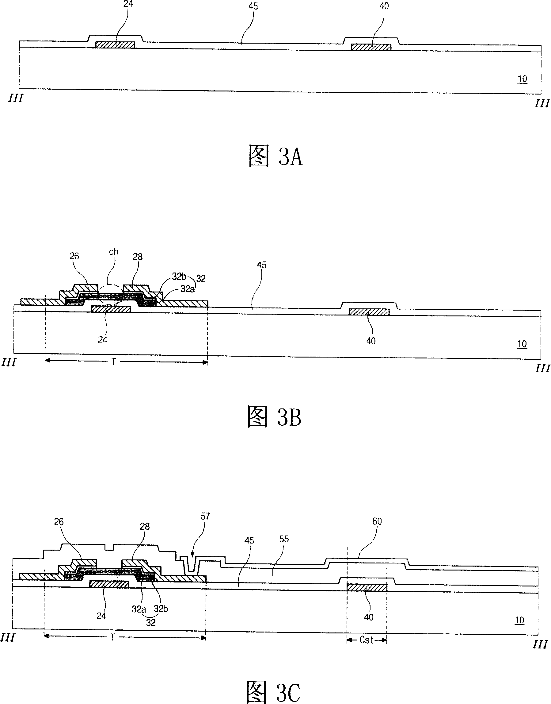
[0035] 5 is a schematic plan view of an array substrate for an LCD device according to an exemplary embodiment of the present invention, FIG. 6 is a cross-sectional view of two pixel regions in the region "VI" of FIG. 5 according to an exemplary embodiment of the present invention, and FIG. 7 is A cross-sectional view of region "VII" of FIG. 6 according to an exemplary embodiment of the present invention. In FIGS. 5 , 6 and 7 , a plurality of gate lines 120 are formed on the substrate 100 along a first direction, and a plurality of data lines 130 are formed along a second direction crossing the first direction. The gate line 120 includes first and second gate lines 120a, 120b spaced apart from each other. The first gate 124a extends from the first gate line 120a, and the second gate 124b extends from the second gate line 120b. Here, the fi...


PUM


Abstract

An array substrate for liquid crystal display devices includes first and second gate lines spaced apart from each other, a common line between the first and second gate lines parallel to the first and second gate lines, a data line crossing the first and second gate lines to define first and second pixel regions with respect to the common line, a first thin film transistor at a crossing portion of the first gate line and the data line, a second thin film transistor at a crossing portion of the second gate line and the data line, a first pixel electrode connected to the first thin film transistor in the first pixel region, and a second pixel electrode connected to the second thin film transistor in the second pixel region, wherein the first and second pixel electrodes have a symmetric shape with respect to the common line.

Description

[0001] This application claims the benefit of Korean Patent Application No. 10-2006-058231 filed in Korea on June 27, 2006, which is incorporated herein by reference in its entirety. technical field [0002] The invention relates to a liquid crystal display (LCD) device, in particular to an array substrate for an LCD device with a high aperture ratio and a manufacturing method thereof. Background technique [0003] In general, LCD devices display images using optical anisotropy and polarity characteristics of liquid crystal molecules. The elongated liquid crystal molecules have directionality. The alignment direction of the liquid crystal molecules can be controlled by applying an electric field to the liquid crystal molecules. As the intensity of the electric field changes, the alignment of the liquid crystal molecules changes accordingly. Since the refraction of incident light passing through the liquid crystal depends on the orientation of liquid crystal molecules, imag...

Claims


Application Information

Patent Timeline
Patent Type & Authority Applications(China)
IPC IPC(8): G02F1/1362G02F1/133H01L21/00
CPCG02F2001/134345G02F1/136286G02F2201/40G02F1/134345G02F1/136
Inventor 权起莹黄光熙
Owner LG PHILIPS LCD CO LTD
Why Eureka
Try Eureka