Novel self-filtering narrow spectral response organic light detector

A photodetector and narrow spectrum technology, applied in the field of new self-filtering narrow spectrum response organic photodetectors, can solve the problem of low photon and charge utilization, not paying attention to the band gap relationship between P-type layer and N-type layer materials, Problems such as poor controllability of light field and charge

Active Publication Date: 2019-12-03
GUANGZHOU GUANGDA INNOVATION TECH CO LTD
View PDF3 Cites 7 Cited by
  • Summary
  • Abstract
  • Description
  • Claims
  • Application Information

AI Technical Summary

Problems solved by technology

However, the above-mentioned device structures are all based on the traditional bulk blended heterojunction structure, that is, the P-type electron donor material and the N-type electron acceptor material are blended together as the active layer, and this blended active layer has a great impact on The controllability of the light field and charge is poor, and additional technical means need to be added at the same time to regulate the quantum efficiency or light field distribution in the active layer, such as making an ultra-thick active layer of more than 2 microns to control charge transmission and collection, inserting ultra-thick The thin metal layer is made into an optical microcavity structure, or an ultra-high bias voltage is applied to achieve a narrow spectral response function. However, this kind of organic photodetector based on a bulk heterojunction structure mixed with donors and acceptors usually has a high dark current. , low responsivity, low detectivity, and requires strict technical means to achieve narrow spectral response function, and there are few organic optoelectronic materials suitable for this device structure that can achieve narrow spectral response, making it universal It is difficult to realize the free selection of the detection spectrum band and the free adjustment of the half-peak width of the detection spectrum through a single device structure, which limits its practical application.
In addition, there are recent reports in the literature that try to use P and N layered device structures to achieve narrow response detection [J. Mater. The layer is also made of a variety of P-type layer materials blended, and it does not pay attention to the band gap relationship between the P-type layer and the N-type layer material, and the band gap of the blended P-type layer materials used is narrower than that of the N-type layer. Layer material, so the incident photons have been completely absorbed by the P-type layer, and only the deep P-type layer material can be used to generate excitons. The N-type layer material only exists as an exciton separation interface and will not contribute to the long-wavelength EQE. This makes the utilization of photons and charges low, so it has only 3% external quantum efficiency (EQE) at -4V bias, and more importantly, this irrational use of excitons makes it work in visible light There is still a high EQE response in the range, that is, the narrow spectral response function in the true sense cannot be realized. At the same time, the matching of this bandgap relationship makes it impossible to realize the detection of spectral band and half-peak width by adjusting the thickness of the N-type layer. adjust

Method used


Image

  • Novel self-filtering narrow spectral response organic light detector
  • Novel self-filtering narrow spectral response organic light detector
  • Novel self-filtering narrow spectral response organic light detector

Examples


Embodiment 1

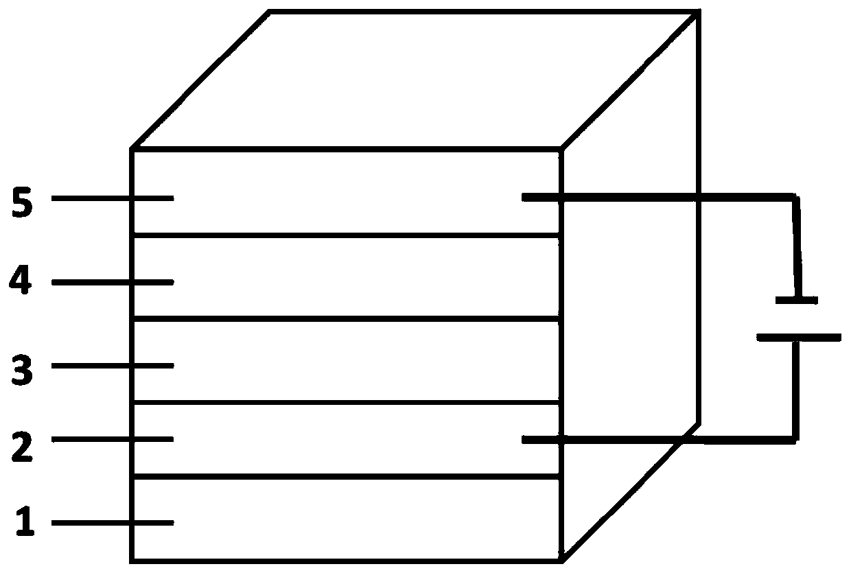
[0115] Such as figure 1 As shown, the novel self-filtering narrow spectral response organic photodetector has a device structure including a substrate 1 , a positive electrode 2 , a P-type layer 3 , an N-type layer 4 and a negative electrode 5 .

[0116] The substrate 1 is glass; the positive electrode 2 is indium tin oxide (ITO); the P-type layer 3 is a single-layer P-type layer structure, and the material of the P-type layer is naphthothiadiazole material NT812, and the film thickness is 1200nm; the material of the N-type layer 4 is a non-fullerene electron acceptor material IEICO-4F, with a film thickness of 150nm; the negative electrode 5 is silver. The band gap of the P-type layer material NT812 is wider than that of the N-type layer material IEICO-4F.

[0117] The preparation method of the above-mentioned organic photodetector comprises the following steps:

[0118] Step 1: Clean the glass substrate sequentially with acetone, special detergent for micron-sized semicond...

Embodiment 2

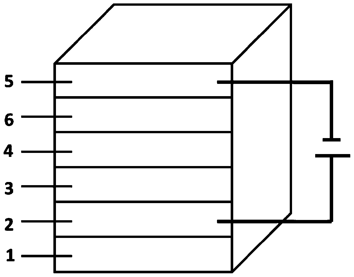
[0124] Repeat embodiment 1, increase buffer layer 6 between its N-type layer 4 and negative electrode 5, specifically as follows: figure 2 As shown, the novel self-filtering narrow spectral response organic photodetector has a device structure including a substrate 1 , a positive electrode 2 , a P-type layer 3 , an N-type layer 4 , a buffer layer 6 and a negative electrode 5 .

[0125] The substrate 1 is glass; the positive electrode 2 is indium tin oxide (ITO); the P-type layer 3 is a single-layer P-type layer structure, and the material of the P-type layer is naphthothiadiazole material NT812; The material of N-type layer 4 is non-fullerene electron acceptor material IEICO-4F, and the film thickness is 150nm; the negative electrode 5 is silver; the buffer layer 6 material is water-alcohol-soluble polymer material [9,9- Dioctylfluorene-9,9-bis(N,N-dimethylaminopropyl)fluorene] (PFN), with a film thickness of 8nm; the bandgap of the P-type layer material NT812 is wider than t...

Embodiment 3

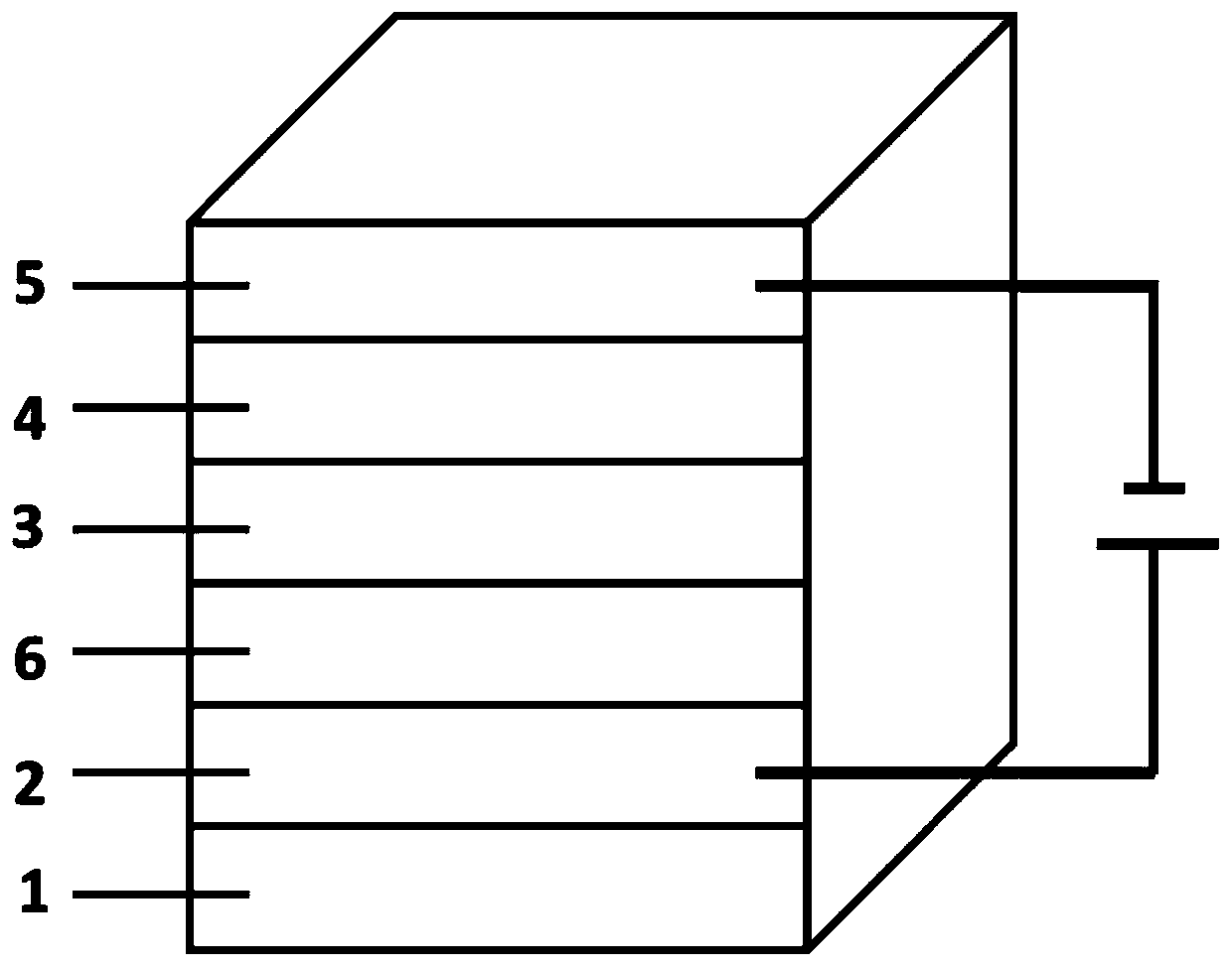
[0135] Repeat embodiment 2, add one deck P-type layer in addition, form multilayer P-type layer structure, specifically as follows: figure 2 As shown, the novel self-filtering narrow spectral response organic photodetector has a device structure including a substrate 1 , a positive electrode 2 , a P-type layer 3 , an N-type layer 4 , a buffer layer 6 and a negative electrode 5 .

[0136] The substrate 1 is glass; the positive electrode 2 is indium tin oxide (ITO); the P-type layer (3) is a multi-layer P-type layer structure, and the first P-type layer material is polythiophene and its derivatives The material is poly(3-hexylthiophene) (P3HT), the film thickness is 150nm, the second P-type layer material is naphthothiadiazole material NT812, the film thickness is 800nm, wherein the second P-type layer is in direct contact with the N-type layer, and the second P-type layer is in direct contact with the N-type layer. A P-type layer is not in direct contact with the N-type layer;...


PUM


Abstract

The invention relates to a novel self-filtering narrow spectral response organic light detector. The organic light detector sequentially comprises a substrate, a positive electrode, a P-type layer, anN-type layer and a negative electrode, the P-type layer can be further divided into a single-layer P-type layer structure and a multi-layer P-type layer structure, and in the single-layer P-type layer structure, the band gap of the P-type layer material is wider than that of the N-type layer material; in the multi-layer P-type layer structure, the band gap of at least one P-type layer material inthe P-type layer materials which are not in direct contact with the N-type layer is wider than that of the N-type layer material and / or the P-type layer material which is in direct contact with the N-type layer, and a buffer layer can be added between the positive electrode and the P-type layer and / or between the N-type layer and the negative electrode. According to the invention, a novel devicestructure and a simple preparation method are adopted, and the free selection of a detection spectrum waveband and the free adjustment of the half-peak width of a detection spectrum are achieved without a band-pass optical filter.

Description

technical field [0001] The invention relates to the field of organic optoelectronics, in particular to a novel self-filtering narrow spectrum response organic photodetector. Background technique [0002] Photodetectors have the function of converting optical signals into electrical signals, and are an important part of imaging systems. They have important applications in many fields such as environmental monitoring, information communication, and biosensing. According to their spectral response bandwidth, photodetectors can generally be divided into wide-response and narrow-response photodetectors. Wide-response photodetectors are usually integrated for polychromatic light detection in low-light conditions, while narrow-response photodetectors are usually applied in monochromatic imaging or visible-blind near-infrared light detection. In recent years, the vigorous development of the field of organic optoelectronics has injected new vitality into the development of organic p...

Claims


Application Information

Patent Timeline
Patent Type & Authority Applications(China)
IPC IPC(8): H01L51/42H01L51/46H01L51/48
CPCH10K71/12H10K30/20Y02E10/549
Inventor 黄飞解博名张凯胡志诚
Owner GUANGZHOU GUANGDA INNOVATION TECH CO LTD
Why Eureka
Try Eureka