Method for producing device

A device and component technology that is used in semiconductor/solid-state device manufacturing, instruments, electrical components, etc., and can solve problems such as pattern deterioration and the inability of light to reach the top of the substrate.

Inactive Publication Date: 2008-01-09
NIKON CORP
View PDF12 Cites 3 Cited by
  • Summary
  • Abstract
  • Description
  • Claims
  • Application Information

AI Technical Summary

Problems solved by technology

[0008] However, in the state where the liquid is filled between the lower surface of the projection optical system and the substrate surface, air bubbles are attached to the lower surface of the projection optical system and the substrate surface, and there are bubbles in the liquid between the projection optical system and the substrate during exposure. If there are bubbles, the light used to form an image on the substrate cannot reach the substrate, or the light used to form an image on the substrate cannot reach the desired position on the substrate, etc., so that the image formed on the substrate Pattern image has deteriorated

Method used


Image

  • Method for producing device
  • Method for producing device
  • Method for producing device

Examples


no. 1 Embodiment

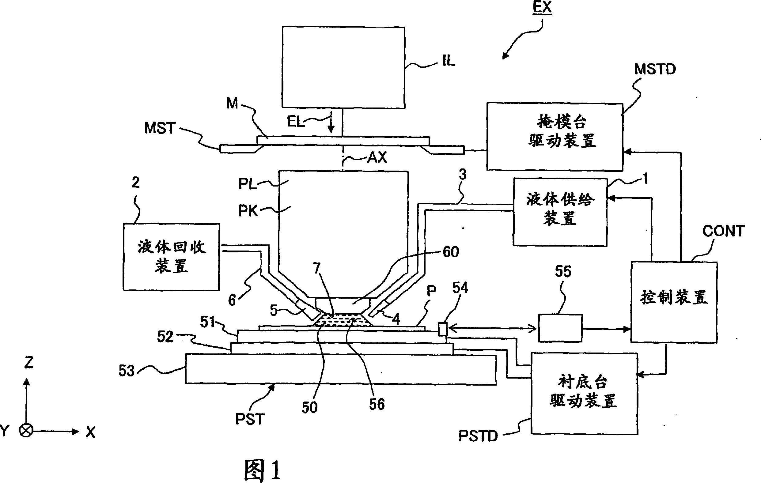
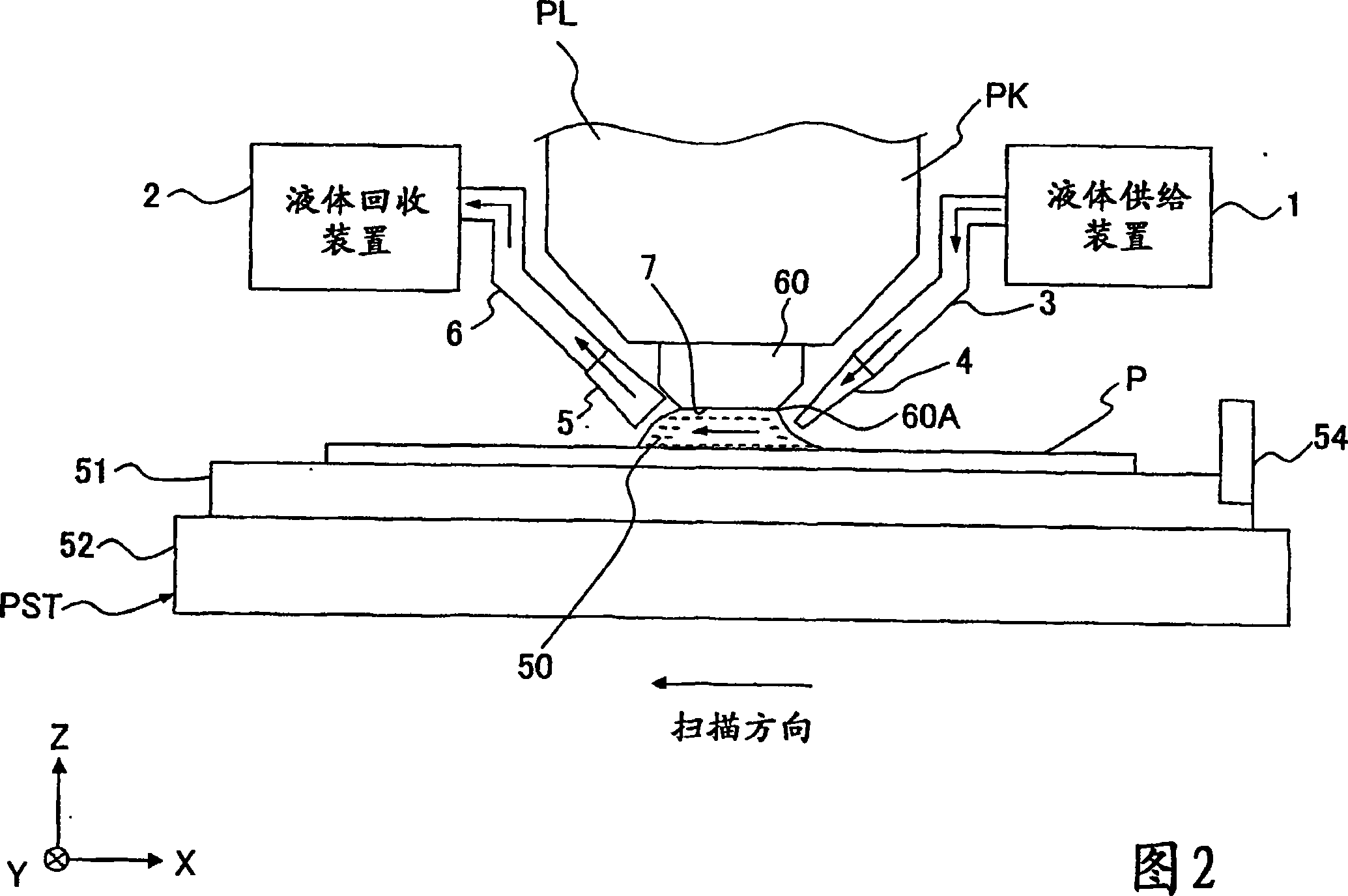
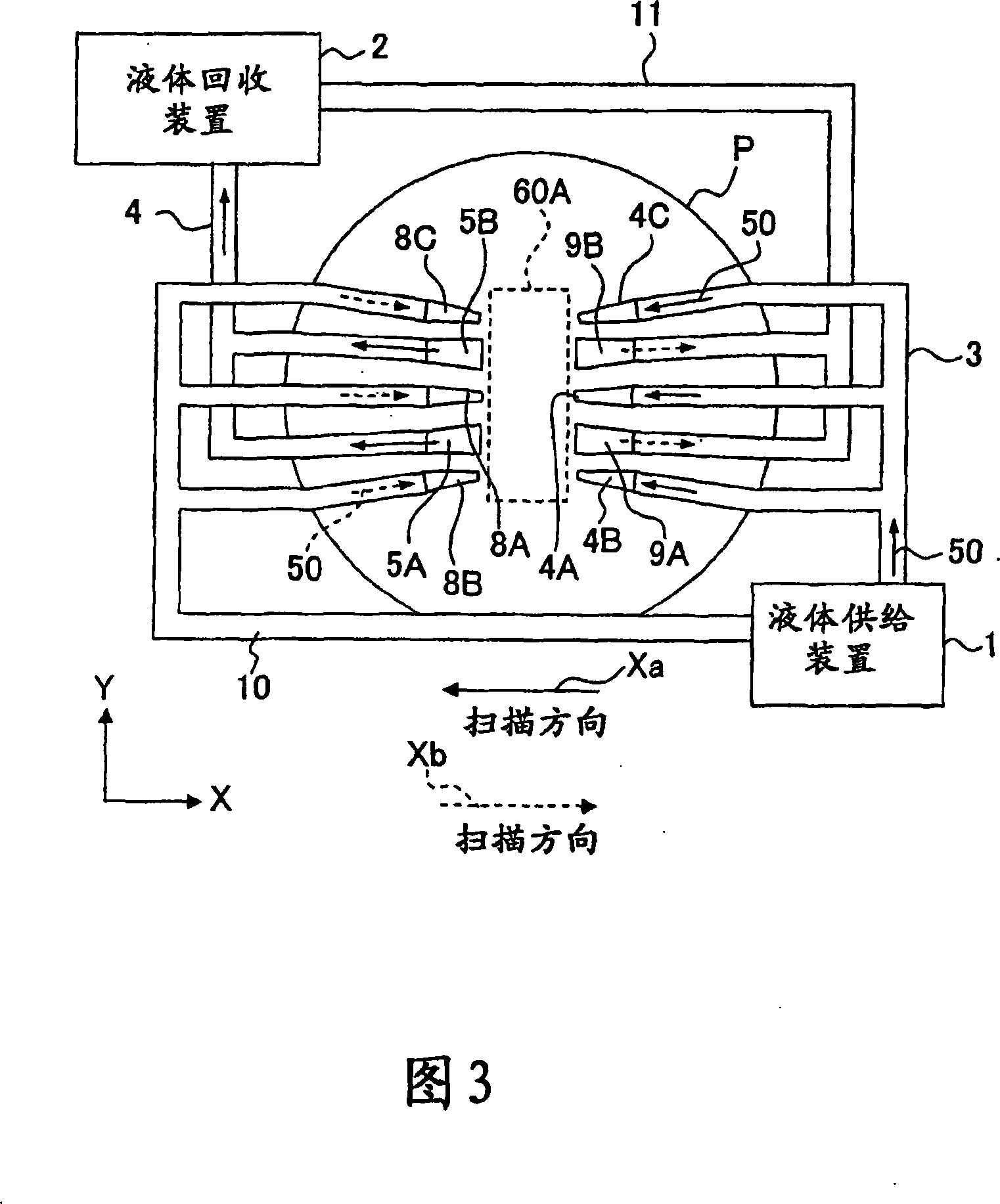
[0039]In FIG. 1 , the exposure apparatus EX includes a mask stage MST for supporting a mask M, a substrate stage PST for supporting a substrate P, and an illumination optical system IL for illuminating the mask M supported by the mask stage MST with exposure light EL. , the projection optical system PL for projecting the pattern image of the mask M illuminated with the exposure light EL onto the substrate P supported by the substrate table PST for exposure, and the control device CONT for overall controlling the overall operation of the exposure apparatus EX.

[0040] Here, for the present embodiment, as an example of the exposure apparatus EX, the mask M and the substrate P are moved synchronously in directions different from each other (opposite directions) to the scanning direction, and the substrate P is exposed and formed on the mask. In the case of a scanning exposure device (so-called scanning stepper) for a pattern on a mold M. In the following description, the directi...

no. 2 Embodiment

[0068] Next, a second embodiment of the exposure apparatus EX of the present invention will be described with reference to FIG. 5 . Here, in the following description, the same or equivalent components as those of the above-mentioned embodiment are given the same reference numerals, and the description thereof will be simplified or omitted. A characteristic part of this embodiment is that a decompression device 23 is provided instead of the heating device 21 .

[0069] As shown in Figure 5, in order to prevent contamination to the substrate P and projection optical system PL, or in order to prevent deterioration of the pattern image projected on the substrate P, the liquid supply device 1 is provided; 50, the filter 20 that removes foreign matter in the liquid 50, the decompression device 23 that degasses the liquid 50 by decompressing the liquid 50 that has removed the foreign matter by the filter 20, and the liquid that has been degassed with the decompression device 23 50 ...

no. 3 Embodiment

[0076] A third embodiment of the exposure apparatus EX of the present invention will be described with reference to FIGS. 6 and 7. FIG. In the exposure apparatus of the present embodiment, a film degassing device 24 and a heating device 25 as shown in FIG. 6 are provided instead of the heating device of the liquid supply device in the first embodiment. In the following description, the same reference numerals are assigned to the same or equivalent components as those of the above-mentioned embodiment, and the description thereof will be simplified or omitted.

[0077] FIG. 6 is a configuration diagram of the liquid supply device 1 . As shown in FIG. 6 , in order to prevent contamination of the substrate P and projection optical system PL, or in order to prevent deterioration of the pattern image projected on the substrate P, the liquid supply device 1 is equipped with: filter the liquid 50 recovered by the liquid recovery device 2, for example. , the filter 20 used to remove ...


PUM

PropertyMeasurementUnit
refractive indexaaaaaaaaaa

Abstract

An exposure apparatus, wherein exposure is carried out while filling a space between a projection optical system and a substrate with a liquid, enables to suppress deterioration of a pattern image caused by any bubble in the liquid. The exposure apparatus includes a liquid supply unit 1 which fills at least a part of the space between the projection optical system and the substrate with a liquid 50 , and exposes the substrate by projecting an image of a pattern onto the substrate via the projection optical system. The liquid supply unit 1 includes a degassing unit 21 which suppresses the generation of the bubble in the liquid 50.

Description

[0001] This application is a divisional application of the patent application with the application number 200380105396.6 (PCT / JP2003 / 015407), the filing date is June 8, 2005, and the invention title is "Exposure Device and Device Manufacturing Method". technical field [0002] The present invention relates to an exposure apparatus for exposing a substrate with a pattern image projected by a projection optical system in a state where at least a portion between the projection optical system and the substrate is filled with liquid, and a device manufacturing method using the exposure apparatus. Background technique [0003] Semiconductor devices and liquid crystal display devices are manufactured by a so-called photolithography method that replicates a pattern formed on a mask onto a photosensitive substrate. The exposure apparatus used in this photolithography process has a mask stage for supporting a mask and a substrate stage for supporting a substrate, and the mask pattern i...

Claims


Application Information

Patent Timeline
Patent Type & Authority Applications(China)
IPC IPC(8): G03F7/20G03F7/00H01L21/027
Inventor 大和壮一
Owner NIKON CORP
Why Eureka
Try Eureka